
Finfet device and fabrication method thereof

a technology of finfet and fabrication method, which is applied in the direction of semiconductor devices, transistors, electrical apparatus, etc., can solve the problems of difficult to further reduce the critical dimension of conventional mosfet, adversely affect the performance of mosfet, and difficult to form finfet devices using existing techniques

Active Publication Date: 2016-07-07
SEMICON MFG INT (SHANGHAI) CORP
View PDF3 Cites 14 Cited by
  • Summary
  • Abstract
  • Description
  • Claims
  • Application Information

AI Technical Summary

Benefits of technology

The existing methods of adjusting the threshold voltages of PMOS and NMOS transistors in a FinFET device involve using work function layers. However, this method has several drawbacks such as the need for multiple mask layers and the inability to effectively adjust the threshold voltage of PMOS transistors. This patent provides an improved FinFET transistor structure and fabrication process to overcome these issues.

Problems solved by technology

Thus, the performance of the MOSFET is adversely affected.
It is often difficult to further reduce the critical dimension of the conventional MOSFET.
However, it may be difficult for the existing techniques to form a FinFET device having PMOS transistors and NMOS transistors with different threshold voltages.

Method used


Image

  • Finfet device and fabrication method thereof
  • Finfet device and fabrication method thereof
  • Finfet device and fabrication method thereof

Examples


Embodiment Construction

[0012]Reference will now be made in detail to exemplary embodiments of the invention, which are illustrated in the accompanying drawings. Wherever possible, the same reference numbers will be used throughout the drawings to refer to the same or like parts.

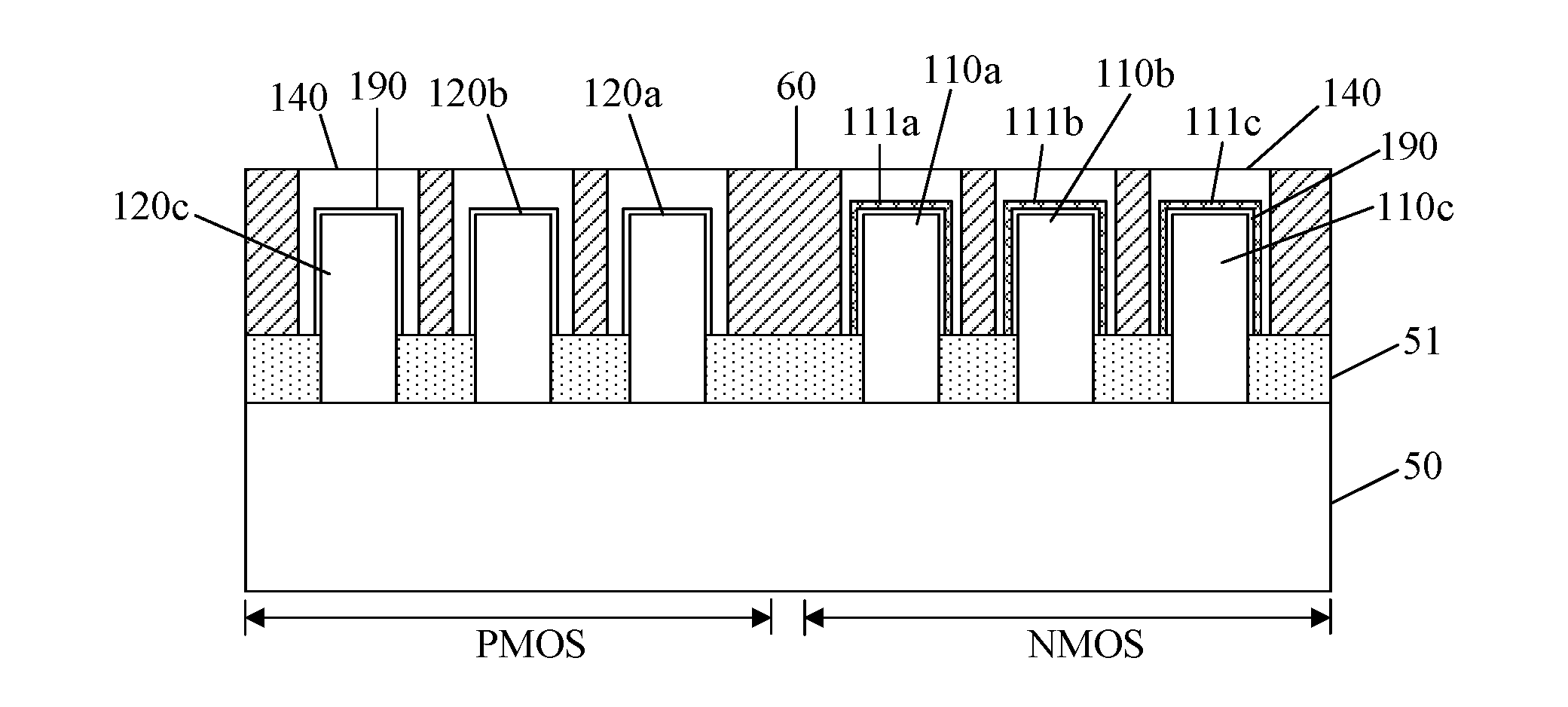
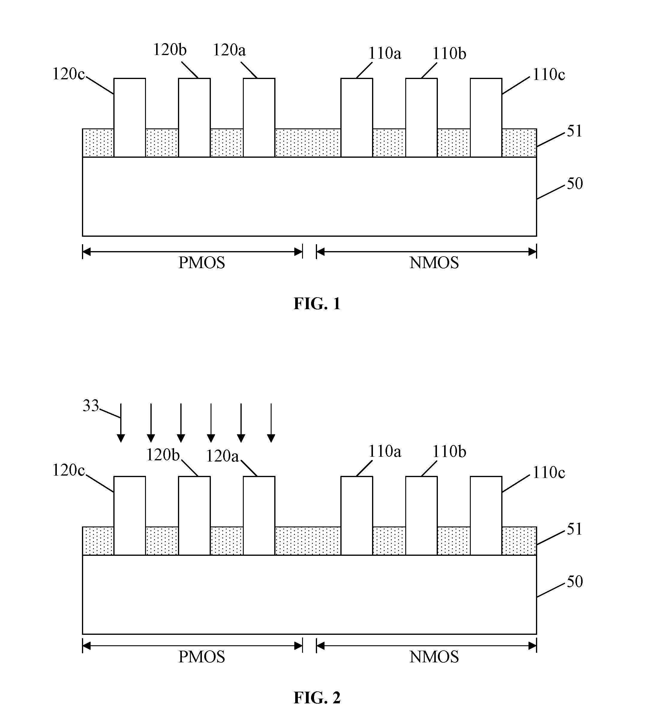
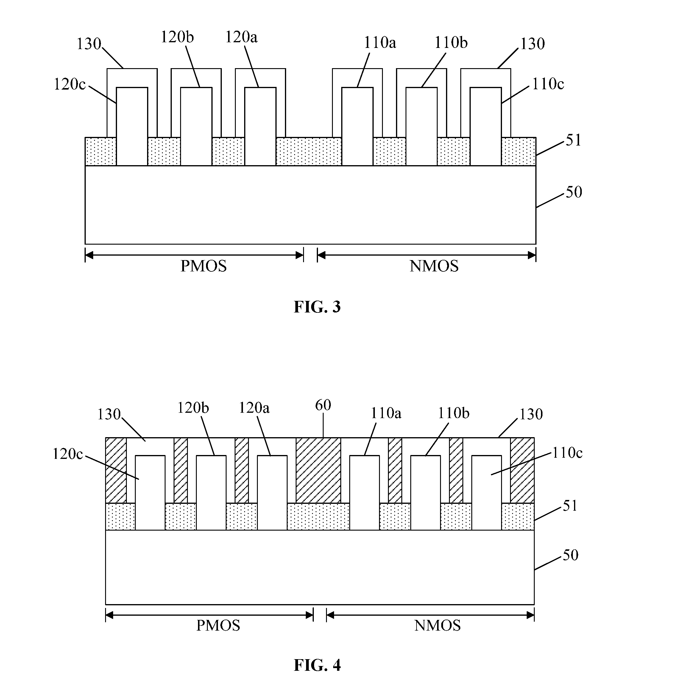
[0013]To form a plurality of PMOS transistors having different threshold voltages and a plurality of NMOS transistors having different threshold voltages in a FinFET device, a commonly used technique is to dope the fins of the FinFET device to cause the PMOS transistors to have different threshold voltages and the NMOS transistors to have different threshold voltages. The critical dimension of the transistors has become smaller and smaller, it may be more and more difficult to dope the increasingly smaller fins to change the threshold voltages of the transistors. The doping resolution may be adversely affected. Thus, the accuracy of the threshold voltage adjustment may be reduced. Further, it may also reduce the stability of the ch...


PUM


Abstract

A method for forming a FinFET device is provided. The method includes providing a substrate having a first region and a second region; and forming a plurality of fins on the substrate. The method also includes forming a plurality of doping regions with different doping concentrations in the fins in the first region; and forming a plurality of dummy gate structures over the plurality of fins. Further, the method includes forming source and drain regions in the plurality of fins at both sides of the dummy gate structures; and removing the dummy gate structures to form a plurality of openings to expose the plurality of fins. Further, the method also includes forming a plurality of work function layers with different work functions on the exposed fins in the openings in the second region; and forming gate structures in the openings.

Description

CROSS-REFERENCES TO RELATED APPLICATIONS[0001]This application claims the priority of Chinese patent application No. 201510005573.8, filed on Jan. 6, 2015, the entirety of which is incorporated herein by reference.FIELD OF THE INVENTION[0002]The present invention generally relates to the field of semiconductor manufacturing technology and, more particularly, relates to FinFET devices and fabrication processes thereof.BACKGROUND[0003]Usually, the gate of a conventional Metal Oxide Semiconductor Field Effect Transistor (MOSFET) is a planar structure. When the critical dimension of the MOSFET is shrunk to a certain value, the short channel effects of the MOSFET become more prominent. The sub-threshold current and the gate leakage current are increased. Thus, the performance of the MOSFET is adversely affected. It is often difficult to further reduce the critical dimension of the conventional MOSFET.[0004]The multiple-gate MOSFET has a better gate control ability; and is able to inhibit...

Claims


Application Information

Patent Timeline
Patent Type & Authority Applications(United States)
IPC IPC(8): H01L21/8238H01L27/092
CPCH01L21/823821H01L21/823857H01L21/823828H01L27/0924H01L21/823842
Inventor JU, JIANHUA
Owner SEMICON MFG INT (SHANGHAI) CORP
Learn More