
Low offset input circuit and transmission system with the input circuit

Inactive Publication Date: 2009-12-10
HITACHI LTD
View PDF7 Cites 11 Cited by
  • Summary
  • Abstract
  • Description
  • Claims
  • Application Information

AI Technical Summary

Benefits of technology

[0009]In view of these circumstances, an object of the present invention is to provide a low offset input circuit and a transmission system which can accommodate a high-speed interface and can achieve reduction of an offset voltage. Another object of the present invention is to provide a low offset input circuit and a signal transmission system which can accommodate a high-speed interface and can adjust an offset voltage in a short time. Note that, the above and other objects and novel characteristics of the present invention will be apparent from the description of the present specification and the accompanying drawings.
[0011]A low offset input circuit according to a typical embodiment of the present invention is mounted on a receiver circuit of a high-speed transmission system including a transmitter circuit, a receiver circuit, and a transmission line, has two operation modes of an input circuit offset voltage detecting operation and an input circuit normal operation, and includes an input circuit block and an offset voltage compensating circuit block. In the input circuit offset voltage detecting operation, as means for directly detecting an offset voltage of the input circuit, variation compensation of the input circuit block is performed by performing short-circuiting between differential input nodes of the input circuit, directly detecting and holding an offset voltage of the input circuit in the offset voltage compensating circuit block, and performing negative feedback of the held offset voltage to the input circuit block. Thereafter, the operation mode transits to the input circuit normal operation, and the input circuit block performs signal amplification in the state where a variation compensation has been performed. Thus, for example, in a high-speed transmission system of Giga (bps) level or higher, signal amplification with a low offset voltage can be achieved with an adjustment performed in a short time by directly detecting an offset voltage and cancelling the offset voltage according to the directly detected offset voltage.
[0012]Here, the input circuit block includes, more specifically, an input circuit which can operate at a high speed and an adder-subtractor circuit block which subtracts an output signal from the offset voltage compensating circuit block from an output node of the input circuit. Specifically, the offset voltage compensating circuit block includes a detecting circuit block which detects an offset voltage of the input circuit and an adjusting and holding circuit block which holds the detected offset voltage. In the detecting circuit block, after an offset voltage of the input circuit to be detected is amplified, for example, by a low offset voltage amplifier called “Auto-Zero amplifier” or the like, a digital determination (binary determination or polarity determination) is performed by a comparator. In this manner, by performing a digital determination after once amplifying the offset voltage of the input circuit in the low offset voltage amplifier in this manner, a highly precise detection of the offset voltage can be made possible with a simple configuration. Also, by holding the detected offset voltage in the adjusting and holding circuit block in the next stage as a digital value, signal amplification of the low offset voltage can be continuously performed for a long time by performing a single detecting operation without frequently repeating a detecting operation and a normal operation.
[0013]To briefly explain an effect obtained by a representative one of inventions disclosed in the present application, in an input circuit accommodating a high-speed interface, reduction of an offset voltage can be achieved. Also, a time required for reducing the offset voltage can be shortened.

Problems solved by technology

Since it is necessary to always correctly measure eye widths which are time components at an adjustment time of the offset voltage, there is such a problem that the adjustment takes labor and much time is required until the canceling amount is determined.
However, in such a system measuring offset voltages indirectly, since it is not easy to realize high precision of measurement accuracy and the offset voltage is adjusted based upon indirect elements, such a case occurs that it is not converged to a desired adjusted state, which essentially results in increase of adjustment time.
Such a problem becomes more significant according to progress of high speed transmission rate.

Method used


Image

  • Low offset input circuit and transmission system with the input circuit
  • Low offset input circuit and transmission system with the input circuit
  • Low offset input circuit and transmission system with the input circuit

Examples


first embodiment

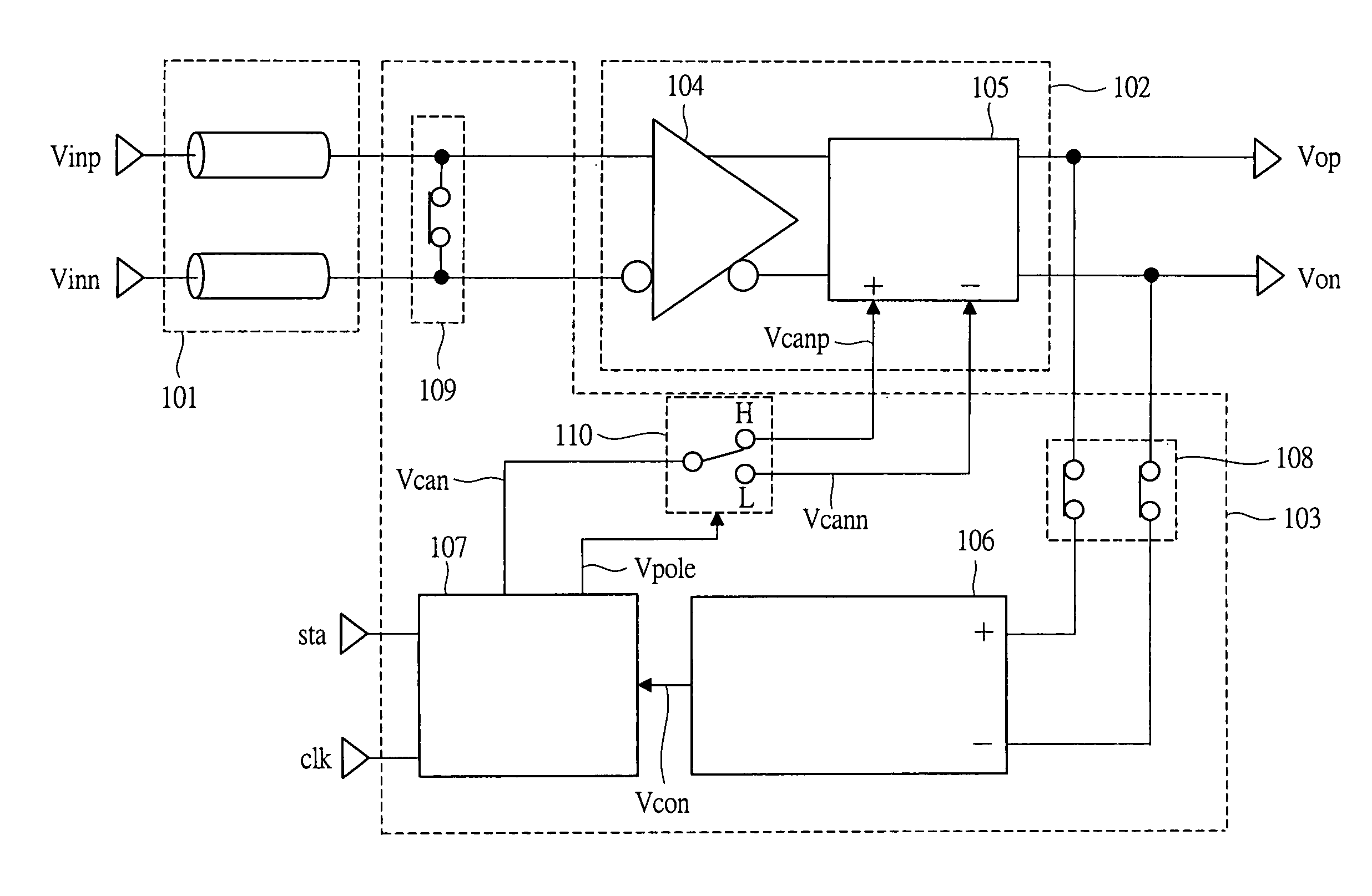
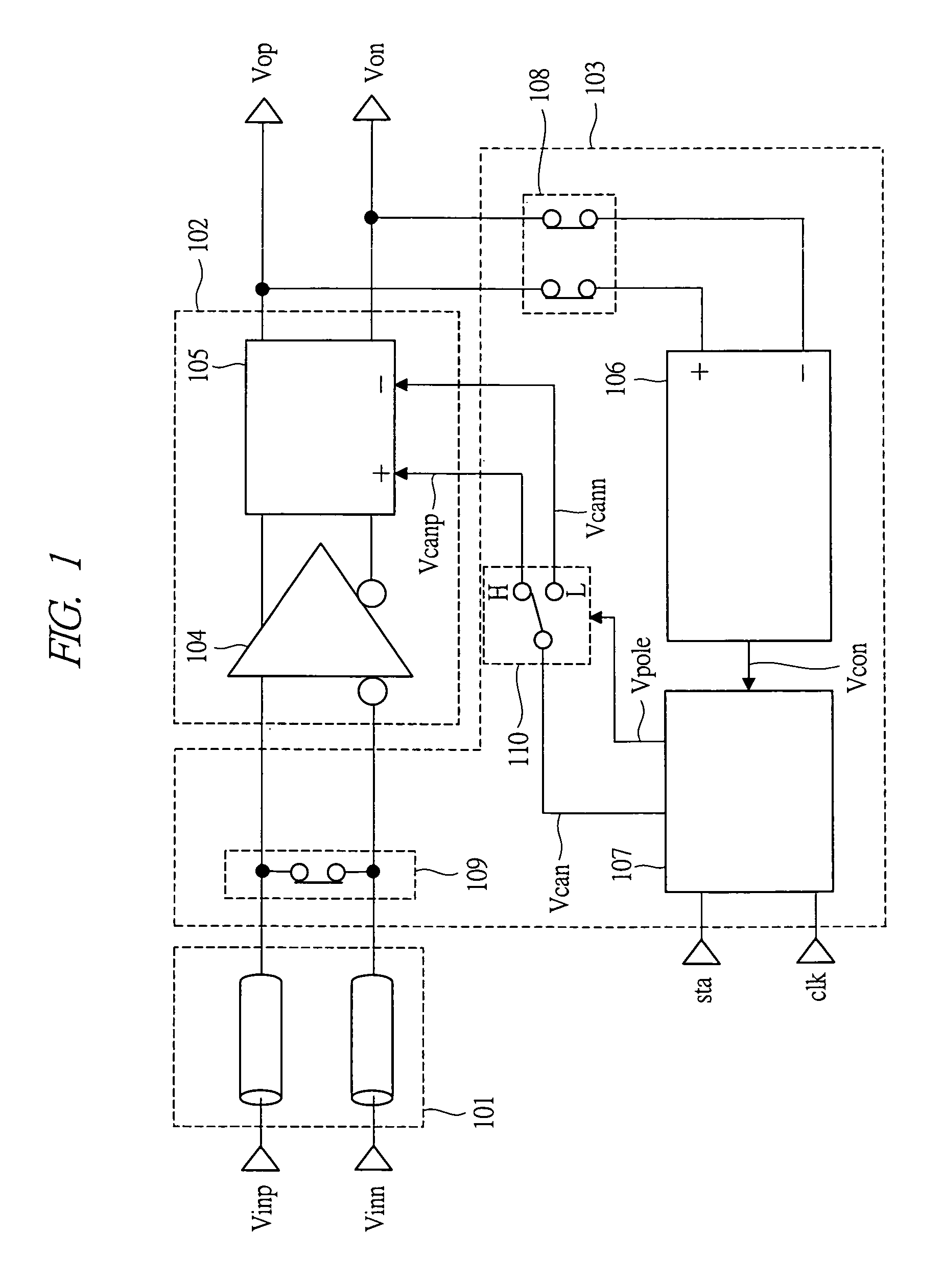
[0037]A low offset input circuit according to a first embodiment cuts off an input circuit from a transmission line by short-circuiting differential input signal terminals of the input circuit; directly detects and holds an offset voltage of the input circuit; and performs negative feedback of the detected amount to the input circuit, thereby reducing the offset voltage of the input circuit. FIG. 1 is a circuit diagram illustrating one example of a configuration of the low offset input circuit according to the first embodiment of the present invention. The low offset input circuit of FIG. 1 has two operation modes of an input circuit offset voltage detecting operation and an input circuit normal operation, and includes an input circuit block 102 which receives a signal from a transmission line 101, and an offset voltage compensating circuit block 103 which reduces an offset voltage of the input circuit block. The input circuit block 102 includes an input circuit 104 which can perfor...

second embodiment

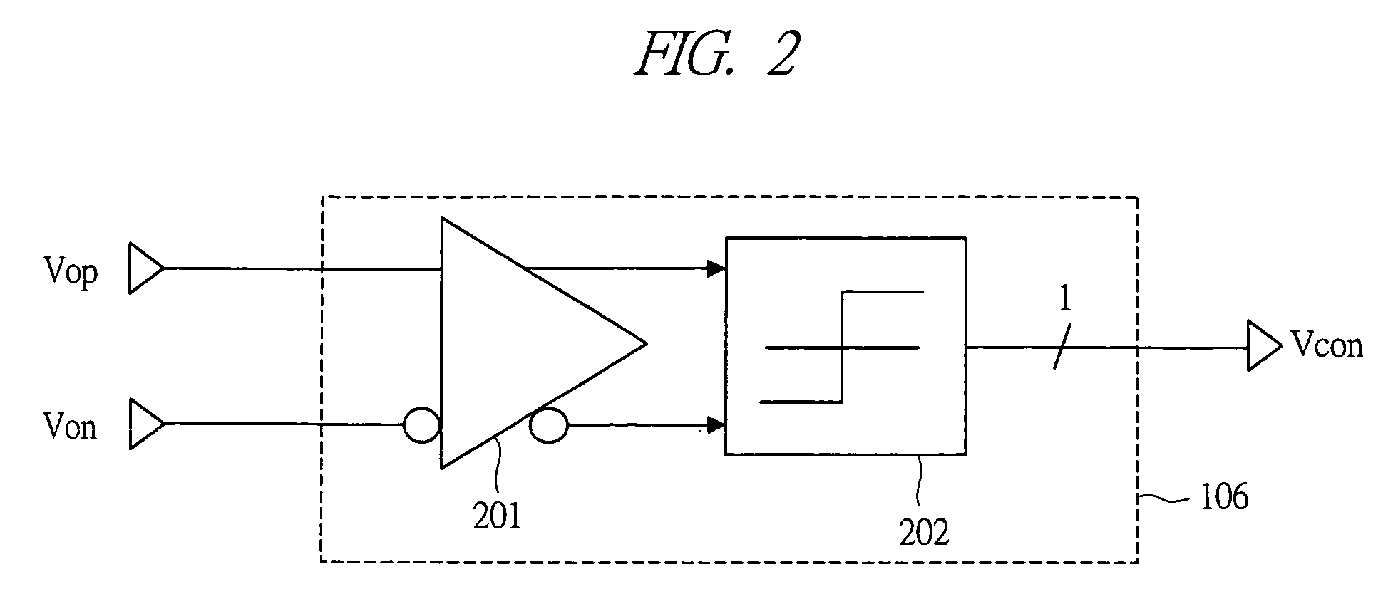
[0040]FIG. 2 is a circuit diagram illustrating one example of a configuration of the detecting circuit block 106 illustrated in FIG. 1 in a low offset input circuit according to a second embodiment of the present invention. The detecting circuit block 106 illustrated in FIG. 2 includes a differential amplifier 201 for a low offset voltage, and a comparator 202. In the present embodiment, variation compensation of the detecting circuit block 106 itself is performed by amplifying an output offset voltage of the input circuit 104 of FIG. 1 in the differential amplifier 201 of a low offset voltage, so that high-precision detection of the offset voltage is made possible. That is, when there is a variation (offset) in the detecting circuit block 106 itself, it is difficult to reduce an output offset voltage of the input circuit 104 with high precision, but such a problem can be solved by using an amplifier having a low offset voltage specification to the differential amplifier 201 in this...

third embodiment

[0042]FIG. 3 is a circuit diagram illustrating a detailed configuration example of the differential amplifier 201 of FIG. 2 in a low offset input circuit according to a third embodiment of the present invention. The differential amplifier 201 illustrated in FIG. 2 is one called “Auto-Zero amplifier” or the like, for example. The Auto-Zero amplifier is a low offset input circuit utilizing sampling, has two operation modes of an auto-zeroing operation and a normal amplifying operation, and includes a high-gain amplifier 301, a sampling capacitor 304, an adder 305, and switches 302 and 303 for selecting one from the abovementioned two operation modes. In the auto-zeroing operation mode, respective switches in FIG. 3 are closed to “L” sides so that an offset voltage of the amplifier 301 is accumulated in the sampling capacitor 304. In the normal amplifying operation, the respective switches are closed to “H” sides, and an input offset voltage accumulated in the sampling capacitor 304 is...


PUM


Abstract

A low offset input circuit and a signal transmission system which can accommodate a high-speed interface and achieve reduction of an offset voltage are provided. An offset voltage compensating circuit block 103 having an input circuit block 108 including an input circuit 104 and an adder-subtractor circuit block 105, switches 108, 109, a detecting circuit block 106, and an adjusting and holding circuit block 107 is provided. To compensate for an offset voltage of the input circuit block 102, an offset voltage of the input circuit block 102 is detected at the detecting circuit block106 by turning on the switches 108, 109, and the detected offset voltage is held in the adjusting and holding circuit block 107, and negative feedback of the held offset voltage to the adder-subtractor circuit block 105 is performed. Thereby, signals Vop, Von having compensated offset voltages are outputted from the input circuit block 102.

Description

CROSS-REFERENCE TO RELATED APPLICATION[0001]The present application claims priority from Japanese Patent Application No. JP 2008-142491 filed on May 30, 2008, the content of which is hereby incorporated by reference into this application.TECHNICAL FIELD OF THE INVENTION[0002]The present invention relates to an input circuit and a transmission system for a high-speed interface of a semiconductor integrated circuit, and in particular, the present invention relates to a circuit technique effective to reduce an offset voltage generated due to variation in device characteristic of an input circuit.BACKGROUND OF THE INVENTION[0003]FIG. 18A is a diagram illustrating a general configuration of high-speed serial transmission between LSIs in an information device typified by a computer or a network device. The configuration includes an output driver 1501 within a transmitter circuit, a transmission line 101, and an input circuit 104 within a receiver circuit, where the input circuit 104 outpu...

Claims


Application Information

Patent Timeline
IPC IPC(8): H04B3/00
CPCH03F3/24H03F3/3028H03F3/45183H03F3/45475H03F3/45605H03F2203/45726H03F2200/411H03F2200/537H03F2203/45212H03F2203/45674H03F2203/45702H03F3/45977
Inventor TAKEMOTO, TAKASHIYAMASHITA, HIROKIYAGYU, MASAYOSHI
Owner HITACHI LTD
Learn More