Solid-state imaging device and imaging device

a technology of imaging device and solid-state imaging, which is applied in the field of solid-state imaging device and imaging device, can solve problems such as degrading image quality, and achieve the effects of reducing impedance, reducing streaking, and improving picture quality

Active Publication Date: 2016-07-14
PANASONIC SEMICON SOLUTIONS CO LTD
View PDF0 Cites 22 Cited by
  • Summary
  • Abstract
  • Description
  • Claims
  • Application Information

AI Technical Summary

Benefits of technology

[0018]The present invention can achieve a solid-state imaging device having the above characteristic configuration, and also an imaging device equipped with this solid-state imaging device.
[0019]The solid-state imaging device and the imaging device of the present invention reduce impedance between the ramp generation circuit and the comparator, and can thus reduce streaking. Accordingly, the present invention can improve the picture quality.

Problems solved by technology

In the CMOS image sensor, if there is a region that has large local luminance difference in an imaging region, the operation of a comparator in the column, including this luminance difference, induces error in A / D conversion in other comparator in a region with other luminance difference, resulting in degrading the image quality.

Method used


Image

  • Solid-state imaging device and imaging device
  • Solid-state imaging device and imaging device
  • Solid-state imaging device and imaging device

Examples


first exemplary embodiment

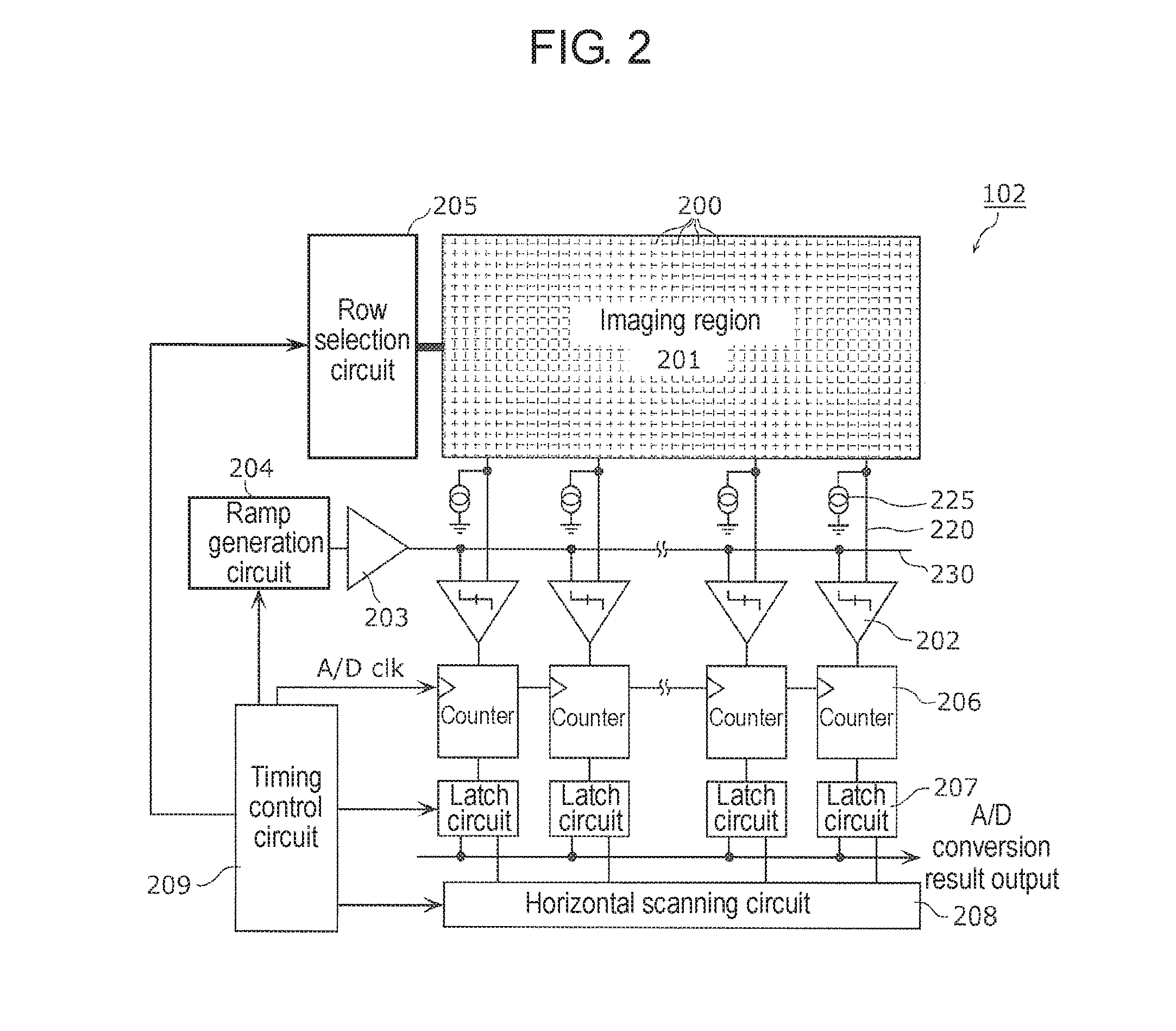
[0036]A solid-state imaging device in the first exemplary embodiment has a configuration of a CMOS image sensor of single-slope column-parallel A / D conversion type.

[0037]FIG. 1 is an example of the configuration of the imaging device (camera) in the first exemplary embodiment. FIG. 2 is a block diagram of the solid-state imaging device in the first exemplary embodiment.

[0038][Configuration of Imaging Device (Camera)]

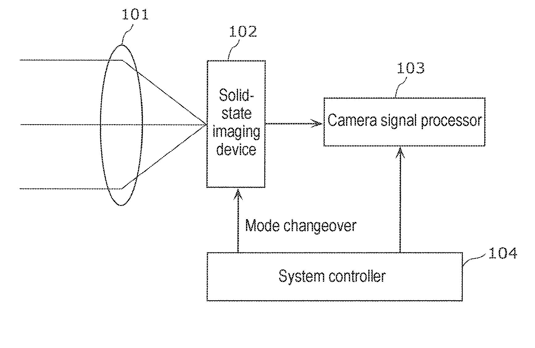
[0039]As shown in FIG. 1, the imaging device (camera) in the exemplary embodiment includes lens 101, solid-state imaging device 102, camera signal processor 103, and system controller 104. Lens 101 is an optical system that guides an incident light to a pixel region of solid-state imaging device 102 (forms an image of subject). For example, it is a lens that forms an image of the incident light (image light) on an imaging face.

[0040]Solid-state imaging device 102 outputs an image signal obtained by converting the image light formed on the imaging face by lens 101 to an e...

second exemplary embodiment

[0075]A solid-state imaging device in the second exemplary embodiment has a configuration of a CMOS image sensor of single slope column-parallel A / D conversion type, same as the solid-state imaging device in the first exemplary embodiment.

[0076][Configuration of Solid-State Imaging Device]

[0077]FIG. 5 is a block diagram of the solid-state imaging device in the second exemplary embodiment. As shown in FIG. 5, solid-state imaging device 112 includes imaging region 201, vertical signal line 220, comparator 202, load current source 225, capacitances CL and CR, ramp buffers 203L and 203R, ramp generation circuits 204L and 204R, row selection circuit 205, counter 206, latch circuit 207, horizontal scan circuit 208, and timing control circuit 209. Solid-state imaging device 112 in FIG. 5 differs from solid-state imaging device 102 in the first exemplary embodiment shown in FIG. 2 with respect to provision of multiple ramp generation circuits and ramp buffers. Solid-state imaging device 112...

modified example

[0090]FIG. 6 is a layout illustrating a floor plan of a modified example of the solid-state imaging device in the second exemplary embodiment.

[0091]As shown in FIG. 6, in solid-state imaging device 122 in the modified example, the ramp circuits 401, 402, 403, and 404 configured with a ramp buffer or ramp buffer and ramp generation circuit are disposed to the left and right so that they are adjacent to comparators 202U and 202D disposed on the top and bottom of imaging region 201. In other words, multiple ramp buffers are provided. Each of multiple comparators 202 simultaneously receive ramp voltage supply from ramp buffers 203L and 203R disposed in plural number. This can reduce wiring impedance of ramp signal lines 221, 222, 223, and 224 from the ramp buffers to input ends of comparators, enabling further reduction of streaking. In this case, reference voltage generation circuits (BGR) 405 and 406 that supply reference voltage or reference current to ramp circuits 401 to 404. The r...


PUM


Abstract

A solid-state imaging device that suppresses streaking includes an imaging region in which unit cells are aligned in matrix, an A/D converter for converting an analog signal generated in the imaging region to a digital signal, and a ramp buffer having an input terminal and an output terminal. Ramp voltage is input to the input terminal, and a reference signal having the ramp voltage is output from the output terminal toward the A/D converter. The A/D converter includes a comparator disposed in each column for comparing an analog signal with a reference signal, and a counter disposed corresponding to the comparator for counting a comparison period of the comparator. The ramp buffer includes a feedback circuit for simultaneously outputting the reference signal to the multiple comparators and controlling the amount of current flowing to the output terminal according to the ramp voltage of the reference signal output from the terminal.

Description

TECHNICAL FIELD[0001]The present invention relates to a solid-state imaging device and imaging device.BACKGROUND ART[0002]FIG. 8 is a block diagram of a conventional solid-state imaging device disclosed in PTL1. Solid-state imaging device 500 in the figure includes imaging region 510, row selection circuit 520, horizontal scanning circuit 530, timing control circuit 540, ADC group 550, digital-analog converter (DAC) 560 as a ramp signal generator, amplifier circuit 570, signal processing circuit 580, and horizontal transmission line 590. Single slope column-parallel ADC including comparator 551, counter 552, and latch circuit 553 is aligned in multiple columns in ADC group 550.[0003]Comparator 551 compares ramp voltage Vslope that has stepwise ramp waveform output from DAC 560 via ramp signal line 555 with an analog signal output from pixel per row via vertical signal line 554. Counter 552 counts comparison time of comparator 551. By the above operation of comparator 551 and counter...

Claims


Application Information

Patent Timeline
Patent Type & Authority Applications(United States)
IPC IPC(8): H04N5/357H04N5/3745H04N5/243H04N5/378
CPCH04N5/357H04N5/378H04N5/243H04N5/37452H04N5/37455H04N25/677H04N25/76H04N25/75H04N25/60H04N23/76H04N25/771H04N25/772
Inventor SHISHIDO, SANSHIROHIGUCHI, MASAHIROICHIRYU, DAINISHIMURA, KAZUKOABE, YUTAKA
Owner PANASONIC SEMICON SOLUTIONS CO LTD
Why Eureka
Try Eureka