
Hall element

Active Publication Date: 2016-07-21
ABLIC INC
View PDF2 Cites 8 Cited by
  • Summary
  • Abstract
  • Description
  • Claims
  • Application Information

AI Technical Summary

Benefits of technology

The patent text states that the invention can lead to lower costs and better performance. This means that the chip can be made more efficiently and without compromising its quality.

Problems solved by technology

It is considered that the offset voltage is generated when potential distribution inside the element becomes imbalanced by, for example, mechanical stress applied to the element from the outside or misalignment occurring in a manufacturing process.
In order to detect a vertical magnetic field component (Z direction) and horizontal magnetic field components (X and Y directions) on a substrate (wafer) surface, it is necessary to form a horizontal Hall element and a vertical Hall element on the same substrate, which leads to an increase in chip size.
Thus, the magnetic field components are detected at different positions and accuracy is lost.
In addition, in order to compensate for an offset voltage of the vertical Hall element configured to detect a horizontal magnetic field, it is necessary to arrange a plurality of vertical Hall elements, which leads to drawbacks such as a further increase in chip size and a higher cost.

Method used


Image

  • Hall element
  • Hall element
  • Hall element

Examples


Embodiment Construction

[0031]Now, modes for carrying out the present invention are described in detail with reference to the drawings.

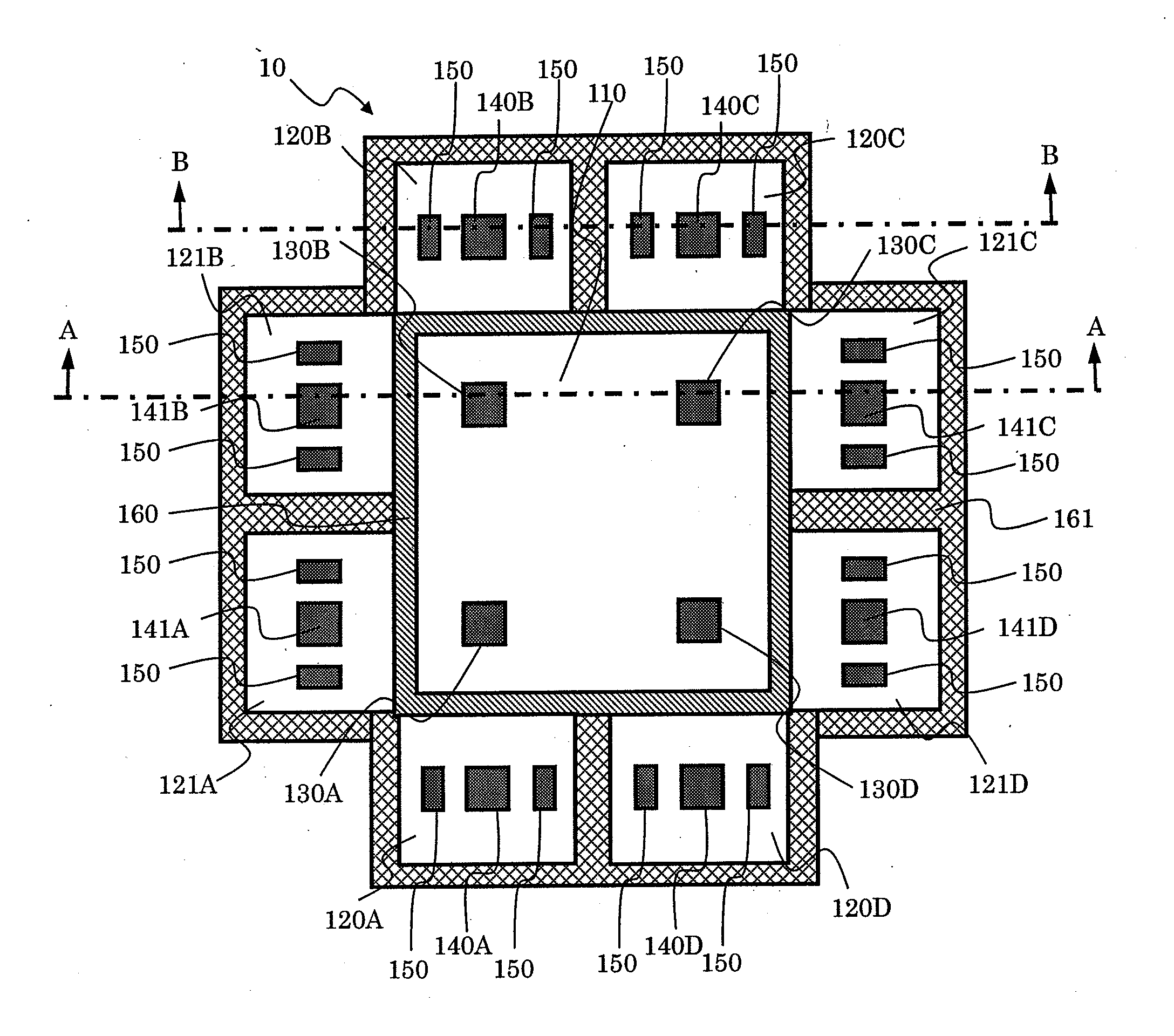
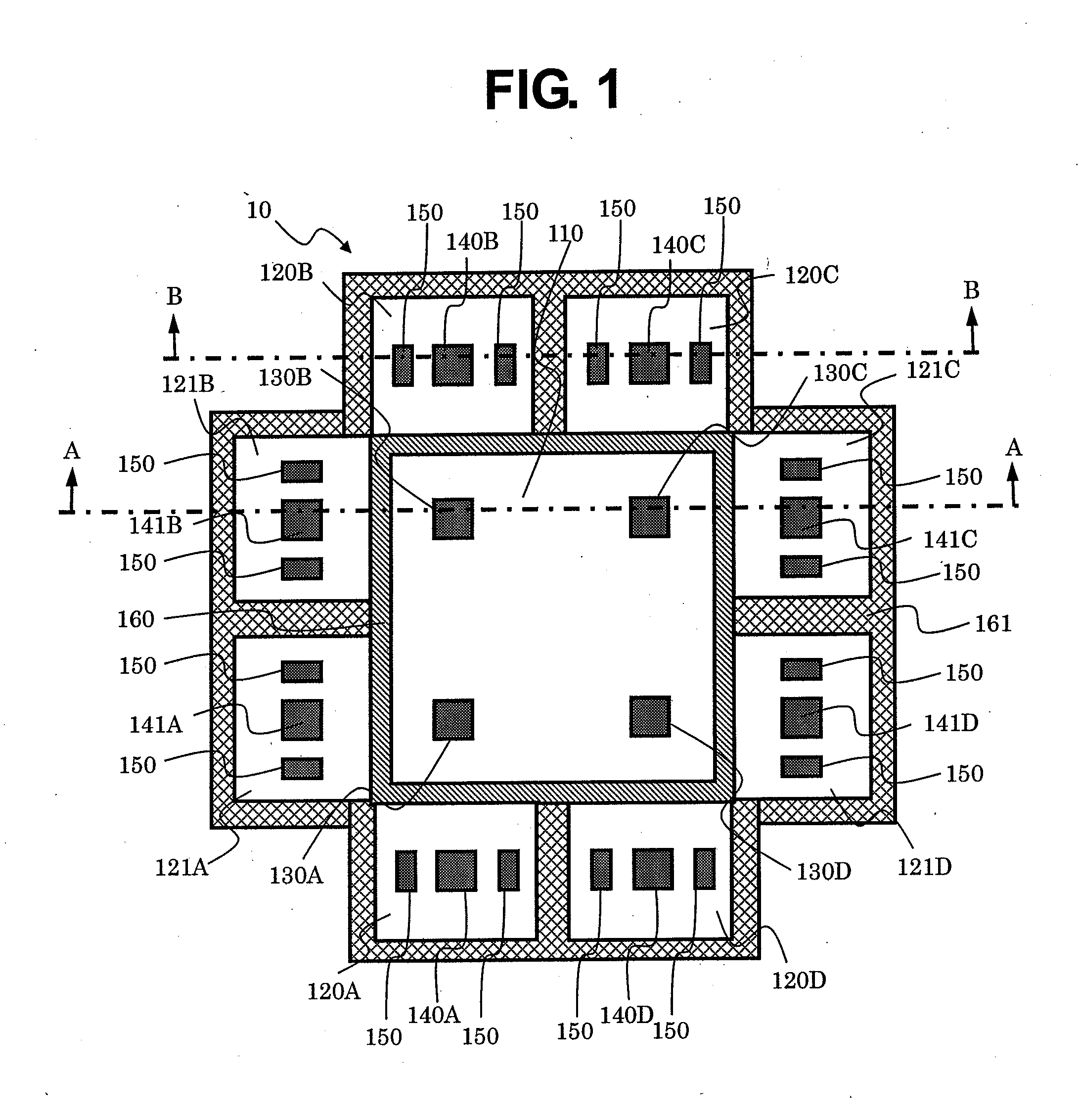
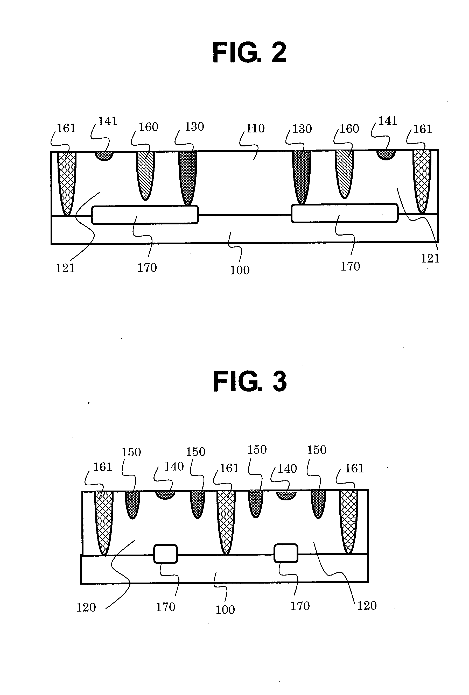
[0032]FIG. 1 is a plan view of a Hall element according to one embodiment of the present invention. FIG. 2 is a vertical cross-sectional structure diagram of the Hall element according to the embodiment of the present invention taken along the line A-A of FIG. 1. FIG. 3 is a vertical cross-sectional structure diagram of the Hall element according to the embodiment of the present invention taken along the line B-B of FIG. 1.

[0033]First, a shape of the Hall element is described.

[0034]As illustrated in FIG. 1 to FIG. 3, a Hall element 10 includes, on a P-type semiconductor substrate layer 100, a vertical magnetic field detection N-type doped region 110 and eight horizontal magnetic field detection N-type doped regions 120A to 120D and 121A to 121D which are configured to detect vertical magnetic field components to a square substrate (wafer) surface, the horizontal magnetic fi...


PUM


Abstract

Provided is a Hall element integrated on a single substrate capable of cancelling offset voltage with a spinning switch configured to switch spinning current and capable of simultaneously detecting a horizontal direction magnetic field and a vertical direction magnetic field. The Hall element has a four-fold rotational axis and includes: a P-type semiconductor substrate layer (100) formed of P-type silicon; a vertical magnetic field detection N-type doped region (110) formed on the P-type semiconductor substrate layer; and eight horizontal magnetic field detection N-type doped regions (120, 121) formed so as to surround the vertical magnetic field detection N-type doped region.

Description

BACKGROUND OF THE INVENTION[0001]1. Field of the Invention[0002]The present invention relates to a semiconductor Hall element, and more particularly, to a Hall element capable of detecting magnetic fields in vertical and horizontal directions and removing offset voltage.[0003]2. Description of the Related Art[0004]A Hall element enables non-contact position detection and angle detection, and is thus used as a magnetic sensor.[0005]First, the principle of magnetic detection by a Hall element is described. When a magnetic field is applied vertically to a current flowing through a substance, an electric field (Hall voltage) is generated in a direction vertical to both the current and the magnetic field.[0006]FIG. 5 is a diagram for illustrating the principle of an ideal Hall effect. On an ideal Hall element, a Hall voltage VH output from a voltmeter 3 is represented as:VH=μB(W / L)Vdd where W and L represent respectively a width and a length of a Hall element magnetism sensing portion 1,...

Claims


Application Information

Patent Timeline
IPC IPC(8): G01R33/07
CPCG01R33/077G01R33/07H10N52/00G01R33/075
Inventor HIOKA, TAKAAKIEBIHARA, MIKA
Owner ABLIC INC
Learn More