Mosfet protection using resistor-capacitor thermal network

a technology applied in the direction of emergency protective circuit arrangement, electronic switching, pulse technique, etc., can solve the problems of long duration current-limit event, load loss, high power dissipation of mosfet, etc., to reduce the number of resistor and capacitor elements, reduce the cost, and model both short and long times accurately

Active Publication Date: 2016-07-28
ANALOG DEVICES INT UNLTD
View PDF2 Cites 13 Cited by
  • Summary
  • Abstract
  • Description
  • Claims
  • Application Information

AI Technical Summary

Benefits of technology

[0022]An additional implementation may include a method to detect the case temperature of the MOSFET. This may reduce the number of resistor and capacitor elements required in the RC thermal model because only the temperature difference between the silicon junction and the case temperature of the MOSFET is modeled. Typically, the time constant from the silicon junction to the case of the MOSFET is between 10 ms and 1 second. If the MOSFET case temperature is not sensed, it may be necessary to include the board temperature behavior in the RC thermal model. This time constant may be several minutes. Modeling both short and long times accurately with a single thermal model requires more resistors and capacitors than representing only shorter times or longer times accurately. Additionally, when modeling both short and long time constants in a single thermal model, the analog multiplier and transconductance amplifier must be accurate over a wide range of power inputs which may be difficult to design. This temperature sensing behavior may be implemented using a resistive divider where the top resistor has a positive temperature coefficient and is electrically connected to the MOSFET drain and is in close proximity on the board. Resistors with accurately specified temperature coefficients are widely available at relatively low cost. This results in a circuit that crosses a threshold (and results in the MOSFET turning off) when the MOSFET case temperature rises above a predetermined temperature.

Problems solved by technology

During this time, the voltage and current through the MOSFET can both be large, resulting in high power dissipation in the MOSFET.
If this power dissipation persists, the MOSFET can reach temperatures that cause damage.
The load will lose power and the hot swap controller will indicate that a fault has occurred.
An even longer time-out setting may be required if another allowable operating condition, such as a fast increase in the input supply voltage or the presence of a load current during start-up, causes an even longer duration current-limit event.
The worst-case condition is not always readily apparent, and determining the worst-case condition is sometimes the most challenging aspect of designing a hot swap circuit.

Method used


Image

  • Mosfet protection using resistor-capacitor thermal network
  • Mosfet protection using resistor-capacitor thermal network
  • Mosfet protection using resistor-capacitor thermal network

Examples


Embodiment Construction

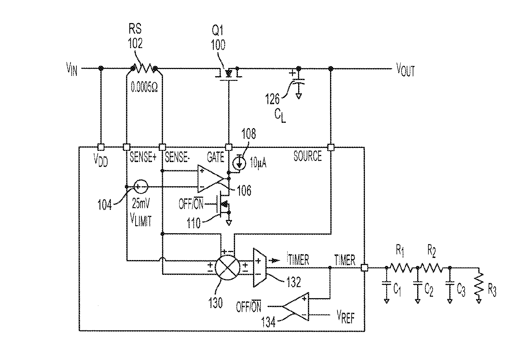
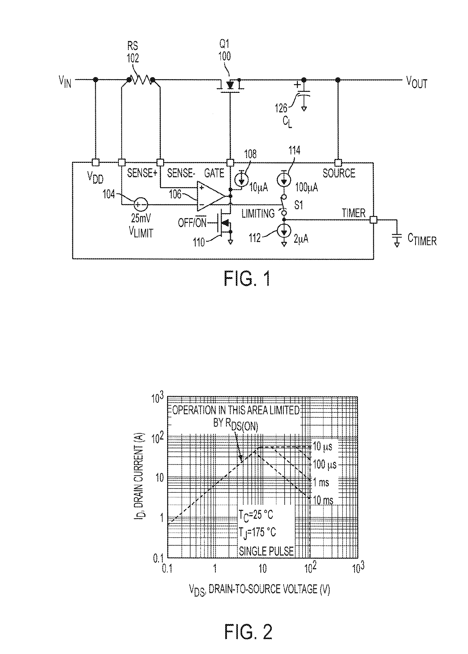
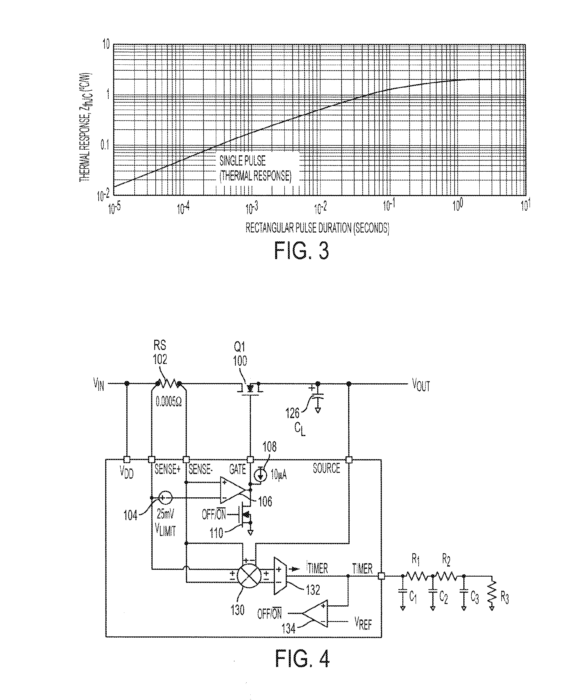
[0033]The present disclosure provides a technique for ensuring that the safe operating area (SOA) of a MOSFET is not exceeded. Historically, the circuit designer has relied on a “safe operating area” (SOA) plot to judge the capability of the MOSFET. An example of the SOA plot reproduced from the Vishay IRF530 datasheet is illustrated in FIG. 2. Cost and physical size of a MOSFET are generally proportional to its SOA capability, so a designer would like to minimize the required safe operating area while safely powering up the output or riding through momentary overload events.

[0034]MOSFET safe operating area is limited by the maximum allowable junction temperature of the MOSFET die. In FIG. 2, the maximum junction temperature is specified as 175° C. when the case temperature is held at 25° C.

[0035]The SOA plot is usually derived from a MOSFET's “transient thermal impedance”. FIG. 3 shows an example of the transient thermal impedance plot reproduced from the Vishay IRF530 datasheet. G...


PUM


Abstract

A circuit for protecting a semiconductor element is provided in a system for supplying power from an input node to an output node. The circuit has an analog multiplier responsive to a voltage across the semiconductor element and a current flowing through the semiconductor element to produce an output voltage. A transconductance amplifier is coupled to an output of the analog multiplier for receiving the output voltage of the analog multiplier to produce an output current. An analog RC circuit coupled to the output of the transconductance amplifier is configurable to include a selected number of resistive elements having selected resistance values and a selected number of capacitive elements having selected capacitance values. The configuration of the RC circuit is carried out to provide an RC thermal model that reproduces a desired thermal behavior of the semiconductor element. The RC circuit is responsive to the output current of the transconductance amplifier to produce an output voltage used to control the semiconductor element.

Description

RELATED APPLICATIONS[0001]This application is a Divisional Application of U.S. Ser. No. 14 / 486,697, filed Sep. 15, 2015, which claims priority of U.S. provisional application No. 61 / 900,832, filed on Nov. 6, 2013. The subject matter of each is incorporated herein by reference in entirety.TECHNICAL FIELD[0002]This disclosure relates to circuits for protecting semiconductor elements in electrical systems. In particular, the disclosure presents ways to protect semiconductor elements, such as MOSFETs, from excessive heating.BACKGROUND ART[0003]A hot swap circuit applies power from an input source to a load in a controlled and protected fashion. One function of such a controller is to limit inrush currents from the power source to the load, especially load capacitance, when power is first applied or if the power source voltage suddenly increases. Another function is to limit current if the load attempts to draw too much current, for example if there is a short circuit in the load.[0004]F...

Claims


Application Information

Patent Timeline
Patent Type & Authority Applications(United States)
IPC IPC(8): H02H5/04H03K17/082
CPCH02H5/04H03K2017/0806H03K17/0822H01C1/16H03K17/08104
Inventor EDDLEMAN, DANIEL JAMESLEE, MITCHELL EDWARDHOU, ZHIZHONG
Owner ANALOG DEVICES INT UNLTD
Why Eureka
Try Eureka