OLED package method and OLED package structure

Active Publication Date: 2016-08-25
TCL CHINA STAR OPTOELECTRONICS TECH CO LTD
View PDF0 Cites 5 Cited by
  • Summary
  • Abstract
  • Description
  • Claims
  • Application Information

AI Technical Summary

Benefits of technology

[0007]An objective of the present invention is to provide an OLED package method, capable of improving the package res

Problems solved by technology

However, the OLED element on the TFT substrate is highly sensitive to the water vapor and the oxygen.
The capability of the present UV package method to resist the water vapor and the oxygen is so poor that the arrangement of the dryer is required to reduce th

Method used


Image

  • OLED package method and OLED package structure
  • OLED package method and OLED package structure
  • OLED package method and OLED package structure

Examples


Embodiment Construction

[0034]Embodiments of the present invention are described in detail with the technical matters, structural features, achieved objects, and effects with reference to the accompanying drawings as follows.

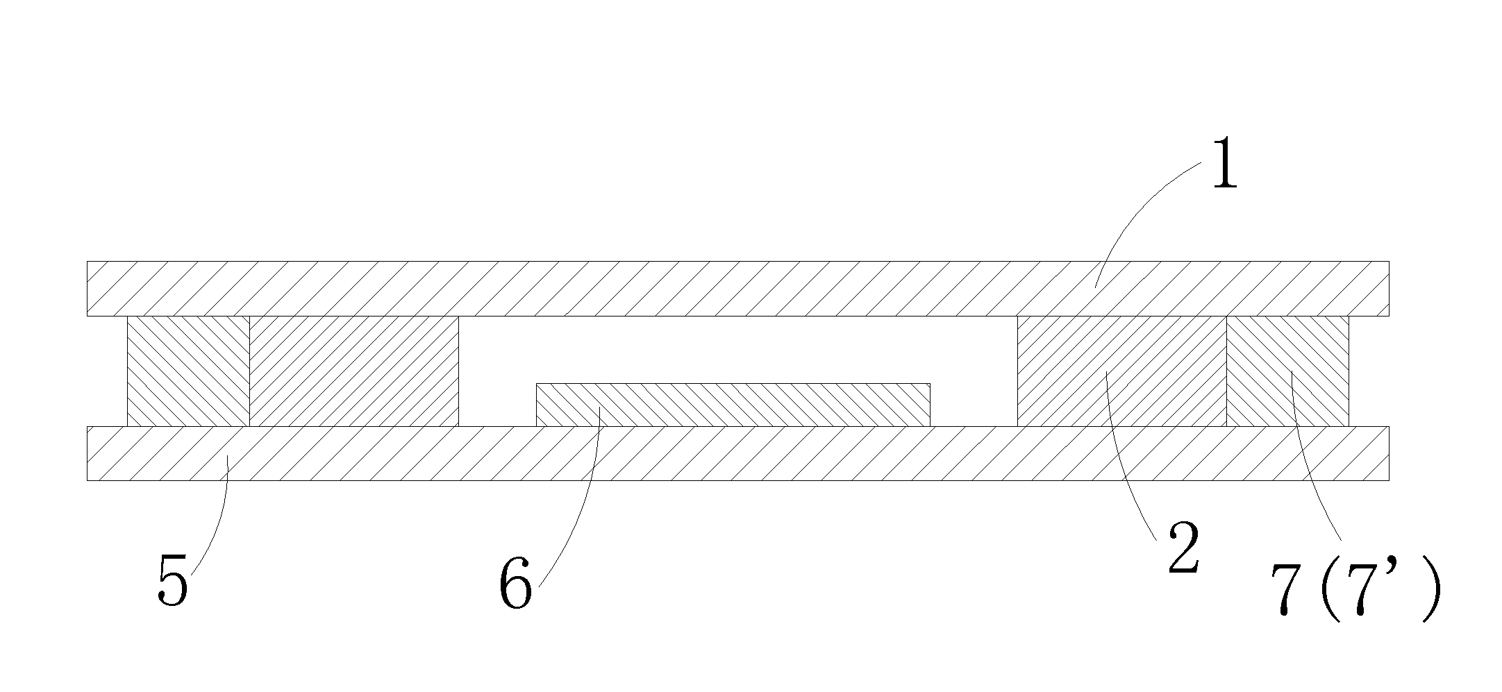
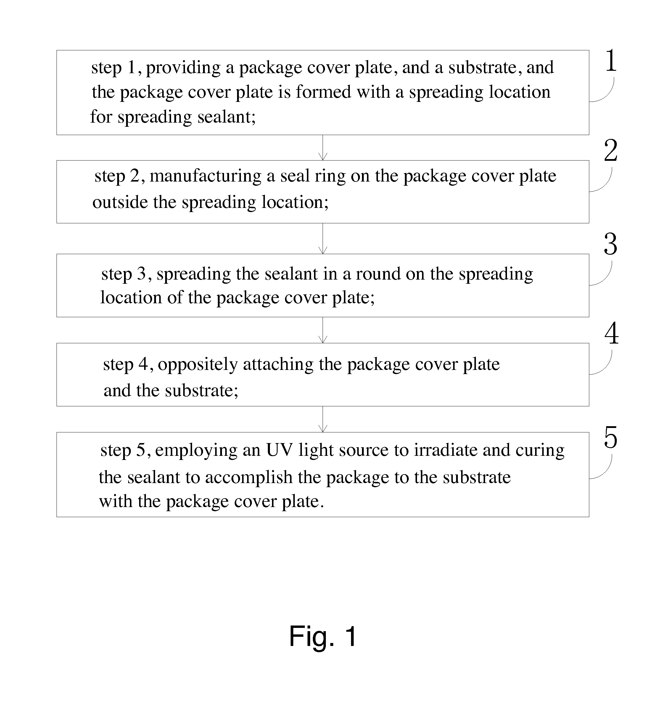
[0035]Please refer from FIG. 1 to FIG. 7. The present invention provides an OLED package method, comprising steps of:[0036]step 1, providing a package cover plate 1, and a substrate 5.

[0037]Preferably, the package cover plate 1 is a glass plate. Preferably, the substrate 5 is a TFT substrate with an LED element 6.

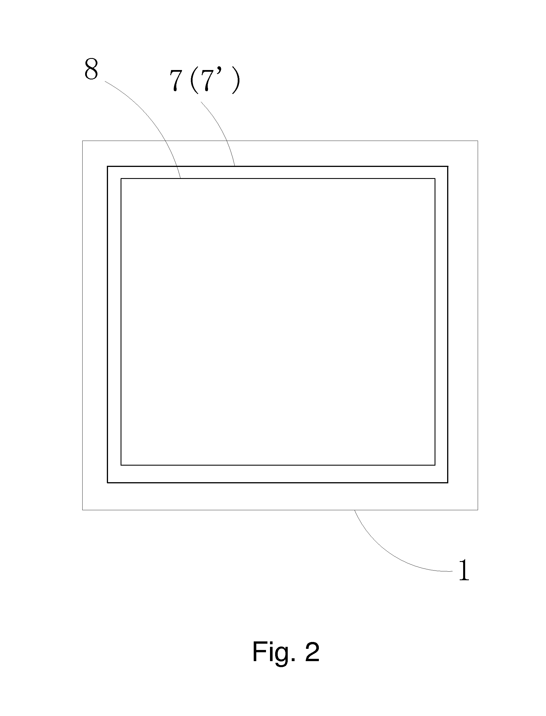
[0038]Specifically, the package cover plate 1 is formed with a spreading location 8 for spreading sealant 2.

[0039]step 2, as shown in FIG. 2, manufacturing a seal ring 7 (7′) on the package cover plate 1 outside the spreading location 8.

[0040]Specifically, as shown in FIG. 3, the seal ring 7 can be an inorganic isolation thin film 3 in a round.

[0041]Specifically, the inorganic isolation thin film 3 is acquired by implementing CVD (Chemical Vapor Deposition) for film formation,...


PUM


Abstract

The present invention provides an OLED package method and an OLED package structure. The method comprises steps of: step 1, providing a package cover plate (1), and a substrate (5), and the package cover plate (1) is formed with a spreading location (8) for spreading sealant (2); step 2, manufacturing a seal ring (7 or 7′) on the package cover plate (1) outside the spreading location (8); step 3, spreading the sealant (1) in a round on the spreading location (8) of the package cover plate (1); step 4, oppositely attaching the package cover plate (1) and the substrate (5); step 5, employing an UV light source to irradiate and curing the sealant (2) to accomplish the package to the substrate (5) with the package cover plate (1).

Description

FIELD OF THE INVENTION[0001]The present invention relates to a display technology field, and more particularly to an OLED package method and an OLED package structure.BACKGROUND OF THE INVENTION[0002]In the display technology field, the flat panel display technologies, LCD (Liquid Crystal Display) and OLED (Organic Light Emitting Diode) have been gradually replaced the CRT (Cathode Ray Tube) displays. The flat light source technology is a new type light source and its skill development has been reached up for the mass production level of the market. In the flat panel display and flat light source technologies, the attachment of two sheet glasses is a very important skill. The package result directly influences the performance of the elements.[0003]The ultra-violet light curing technology is the most earliest and most common skill employed for the LCD / OLED packages. It possesses properties below: no solvent or little solvent is required, which diminishes the pollution of the solvent ...

Claims


Application Information

Patent Timeline
IPC IPC(8): H01L51/52H01L27/32H01L51/56
CPCH01L51/50H01L51/52H01L51/56H01L27/3244H01L2251/558H01L2227/323H01L2251/301H01L2251/303H01L51/5246H10K50/00H10K50/841H10K71/00H10K50/8426H10K2102/351H10K59/12H10K59/1201H10K2102/00
Inventor ZENG, WEIJINGLIU, YAWEI
Owner TCL CHINA STAR OPTOELECTRONICS TECH CO LTD
Why Eureka
Try Eureka