
Pixel Structure and Display Method Thereof, and Display Device

a technology of pixel structure and display method, applied in the field of display, can solve the problems of affecting the display effect, affecting the resolution of the display, and the improvement of the process will reach the limits,

Active Publication Date: 2016-09-01
BOE TECH GRP CO LTD
View PDF2 Cites 39 Cited by
  • Summary
  • Abstract
  • Description
  • Claims
  • Application Information

AI Technical Summary

Benefits of technology

The present invention provides a pixel structure and display method that increases the aperture ratios of sub-pixels, resulting in a brighter and clearer display. Additionally, the display method prevents errors in color edge and color non-uniformity that can occur with traditional pixel arrangements. This improves the display effect of display devices and solves issues related to resolution and process issues in the related art.

Problems solved by technology

Since there is only one color in the direction of column in such an arrangement, the color nonuniformity and the error of color edge are readily to occur, affecting the display effect.
However, the improvement to the process will reach the limits with consistent refinement of the process.
1) The actual display resolution of a display device is the same as the physical resolution thereof. To obtain higher display resolution, it is needed to improve the physical resolution of the display device by increasing the number of sub-pixels. As described above, it is difficult to further increase the resolution when the number of sub-pixels increases up to a certain amount, due to the limit of the improvement to the process;
2) The fact that the number of sub-pixels in a display device is large results in large number of data lines, and thus increases the power consumption of the display device and reduces the aperture ratio of the display device (Generally, the aperture ratio in the art refers to the ratio of the area of light-emitting region in the pixel region and the area of the repeatable pixel unit in the display region. The larger the aperture ratio is, the lower the required brightness of each pixel light-emitting region is and the lower the current density of the brightness of the light-emitting region is so as to achieve the same display brightness). When the resolution is high, it is hard to ensure the aperture ratio of sub-pixel, which may influence on the characteristics of the products, such as lifetime, brightness and the like, consequently.
3) The number of sub-pixels in the display device is large, and the area of each sub-pixel is small, which thus causes the manufacture process of the display device to have great difficulties and high cost. Take the organic light emission display (referred to as OLED) for example, in the related art of manufacturing top-emitting active matrix organic light emission diode (AMOLED), since the fine metal mask (referred to as FMM) usually has limitation to the minimum opening when used for evaporating the pixels arranged in parallel, the sub-pixels with different colors have limitations to the distance between the openings. Thereby, the manufacture process of the display device is inevitably limited to the area of openings of the fine metal mask and the precision of evaporation process, which causes the difficulty in implementing the display device with high resolution.

Method used


Image

  • Pixel Structure and Display Method Thereof, and Display Device
  • Pixel Structure and Display Method Thereof, and Display Device
  • Pixel Structure and Display Method Thereof, and Display Device

Examples


first embodiment

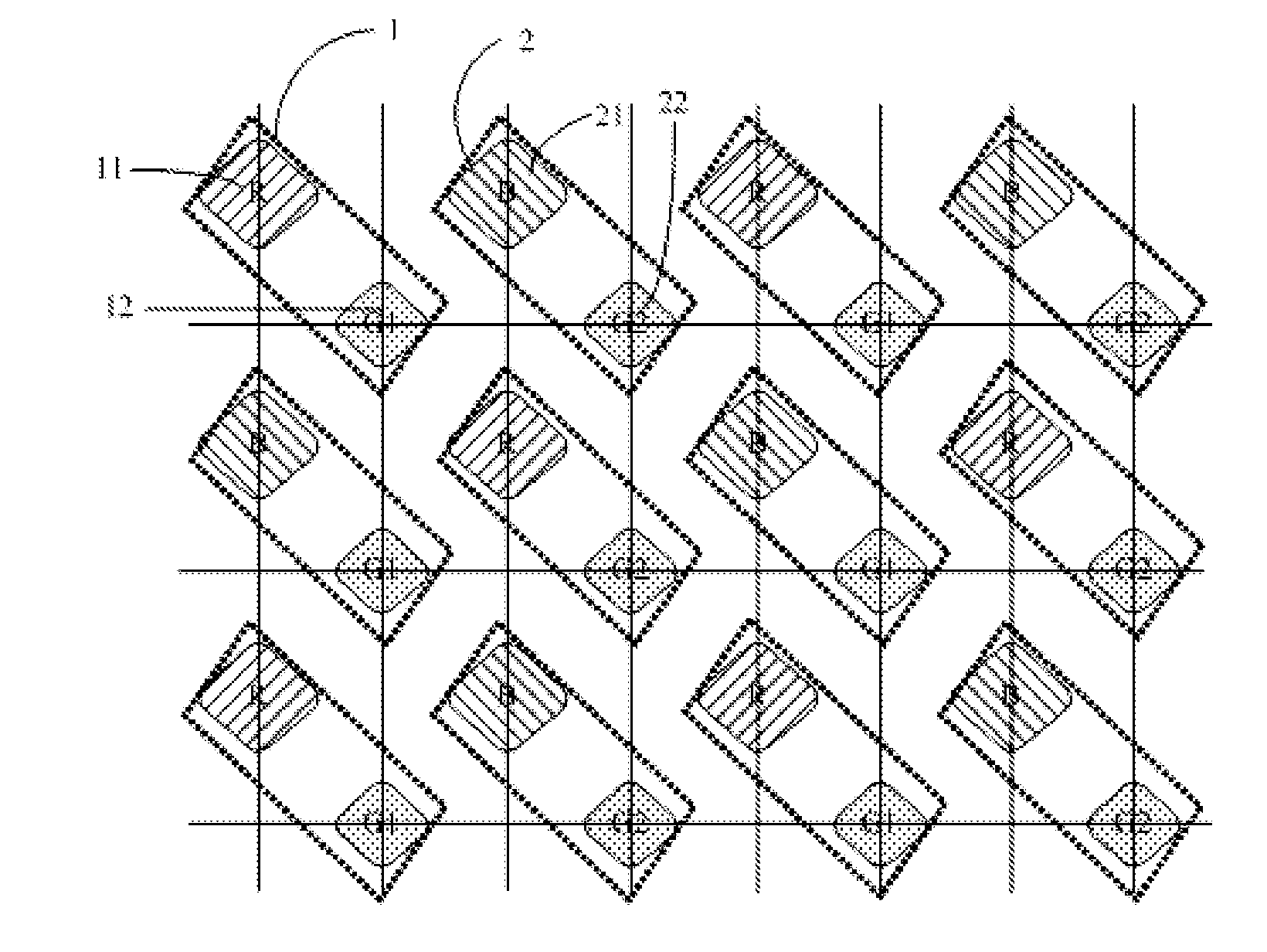
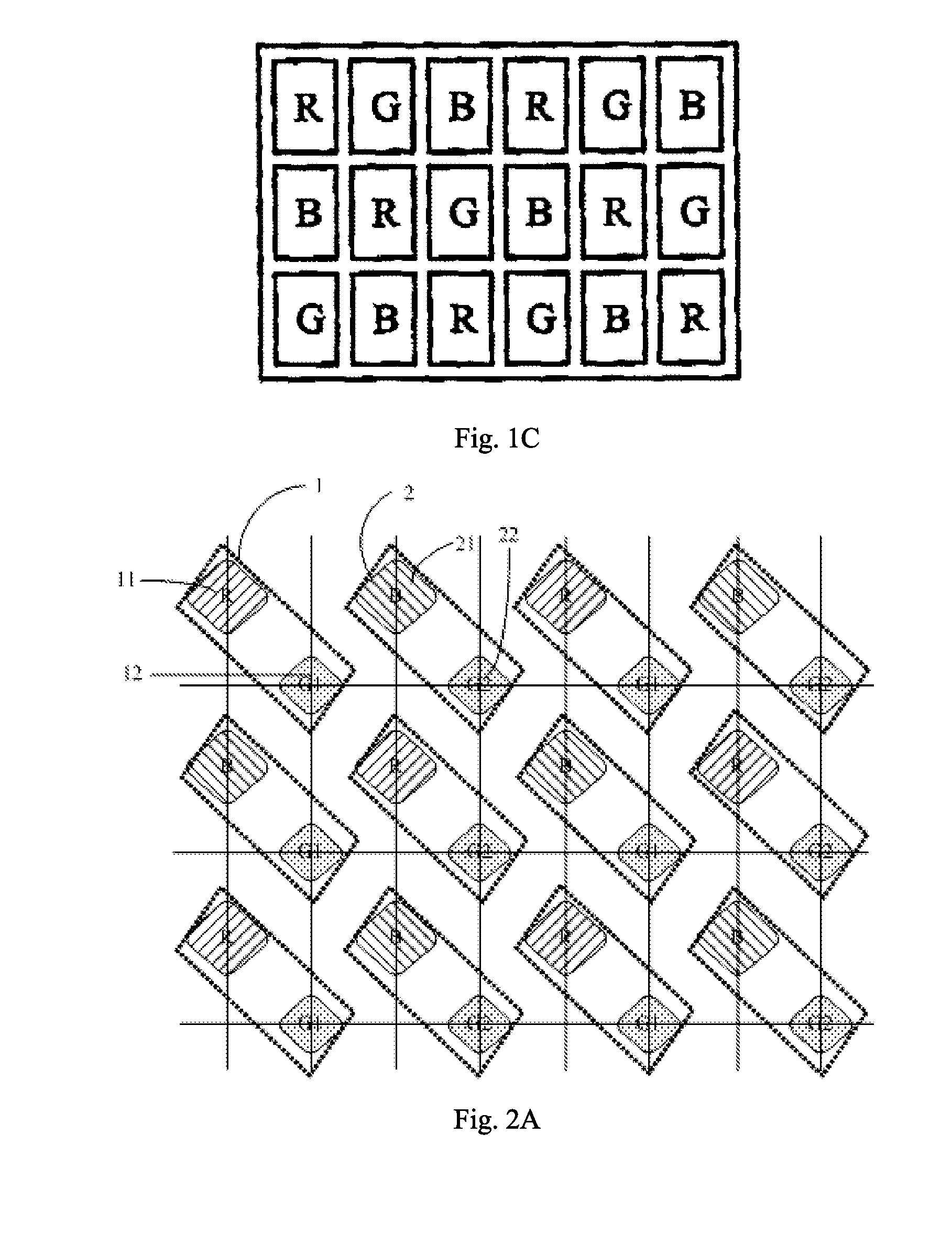
[0060]As shown in FIGS. 2A and 2B, this embodiment provides a pixel structure, including first pixel units 1 and second pixel units 2 which are arranged alternately in turn, wherein the first pixel unit 1 comprises a first sub-pixel 11 and a second sub-pixel 12 arranged in an oblique line, and the second pixel unit 2 comprises a third sub-pixel 21 and a fourth sub-pixel 22 arranged in an oblique line; and the first sub-pixel 11 and the third sub-pixel 21 have different basic colors, and the second sub-pixel 12 and the fourth sub-pixel 22 have the same basic color.

[0061]In this embodiment, the basic color of the first sub-pixel 11 is red, the basic color of the third sub-pixel 21 is blue, and the basic color of the second sub-pixel 12 and the fourth sub-pixel 22 is green. The basic color refers to color owned by the sub-pixel structure and capable of implementing the color display. For example, with respect to the pixel structure in the organic light emitting display device, the basi...

second embodiment

[0089]This embodiment provides a display method of the pixel structure in the first embodiment. In the pixel structure, one pixel unit consists of two sub-pixels and the pixel display with higher resolution may be implemented in conjunction with pixel-sharing algorithm.

[0090]In this embodiment, the first pixel unit 1 additionally uses at least one of the third sub-pixels 21 from adjacent second pixel units 2 to display, and the second pixel unit 2 additionally uses at least one of the first sub-pixels 11 from adjacent first pixel units 1 to display, so that both of the first pixel unit 1 and the second pixel unit 2 can display the pixel display information for sub-pixels of three basic colors.

[0091]In the display, the first pixel unit 1 having a red sub-pixel and a green sub-pixel additionally uses the blue sub-pixel in an adjacent second pixel unit 2 to implement the display of three primary colors of RGB. Similarly, the second pixel unit 2 having a blue sub-pixel and a green sub-p...

third embodiment

[0108]This embodiment provides a display device which uses the pixel structure in the first embodiment and the display method of pixel structure in the second embodiment.

[0109]The display device may be any product or component with the function of display, such as liquid crystal panels, electronic paper, OLED panels, mobile phones, tablet computers, televisions, displays, notebook computers, digital picture frames, navigators and the like.

[0110]The display device shows high yield since the pixel structure thereof is significantly beneficial to the evaporation process for organic layer. Furthermore, the display device shows good display effect for the reason that the pixel structure thereof achieves higher brightness and color uniformity.

[0111]The pixel structure and the display method thereof increases the aperture ratio by improving the pixel arrangement, and correspondingly increases the brightness of pixel structure and the pixel resolution; in the meantime, a display method with...


PUM


Abstract

The invention provides a pixel structure and a display method thereof, and a display device including the pixel structure. The pixel structure comprises first pixel units and second pixel units which are sequentially arranged in staggered positions, wherein the first pixel unit comprises a first sub-pixel and a second sub-pixel arranged in an oblique line, and the second pixel unit comprises a third sub-pixel and a fourth sub-pixel arranged in an oblique line, and wherein the first sub-pixel and the third sub-pixel have different basic colors, and the second sub-pixel and the fourth sub-pixel have the same basic color.

Description

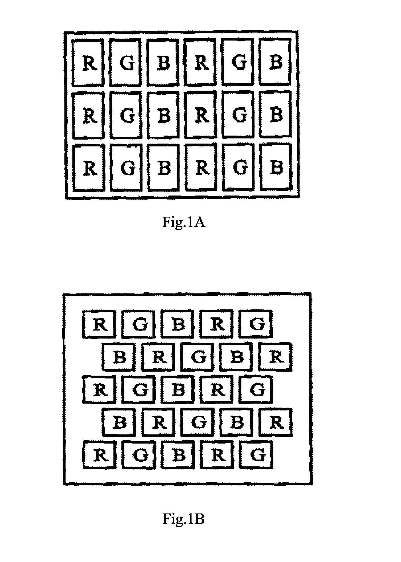
FIELD OF THE INVENTION[0001]The present invention belongs to the technical field of display, and specifically relates to a pixel structure and a display method thereof, and a display device.BACKGROUND OF THE INVENTION[0002]In the flat-panel display devices of the related arts, the color display screen displays an image by means of pixel units. In general, a pixel unit includes sub-pixels with three different colors of red(R), green(G) and blue(B), and the color and brightness displayed in a pixel point (wherein each pixel point corresponds to one pixel unit) are controlled by means of controlling magnitudes of components of three RGB sub-pixels in corresponding pixel unit.[0003]FIGS. 1A to 1C are structural schematic diagrams of arrangements of the RGB sub-pixels in a pixel unit in the related art, including the following three types of arrangement: bar-shape arrangement (see FIG. 1A), delta arrangement (see FIG. 1B) and mosaic arrangement (see FIG. 1C). In FIG. 1A, the RGB sub-pixe...

Claims


Application Information

Patent Timeline
IPC IPC(8): G09G3/20G09G3/3208
CPCG09G3/2003G09G3/3208G09G2320/0242G09G2300/0465G09G2300/0452G02F2201/52H10K59/353G02F1/1362H01L21/32H10K50/00
Inventor WANG, HONGLI
Owner BOE TECH GRP CO LTD
Learn More