Electrical contact

a technology of electric contact and contact plate, which is applied in the field of electric contact, can solve the problems of difficult experimental approaches, unanswered questions regarding the details of the charge transport mechanism of the molecule-electrode interface, and the failure of the fabrication of such devices, etc., and achieves the effects of low viscosity, simple and widely used, and not minimized surface free energy

Active Publication Date: 2016-10-06
NAT UNIV OF SINGAPORE
View PDF0 Cites 4 Cited by
  • Summary
  • Abstract
  • Description
  • Claims
  • Application Information

AI Technical Summary

Benefits of technology

[0048]iii) EGaIn is moldable—which is the ability to shape a material into free-standing, stable structures in which the surface free energy is not minimized. Its moldability may be a function of the ratio of surface area to volume (a ratio which increases as the size of the structure decreases), and is therefore attributable to the properties of its skin. iv) EGaIn is a low-viscosity fluid in the absence of the skin. This low viscosity allows it to be used as an electrically conductive, thermally stable lubricant, and explains why it flows readily—within the confines of its skin—when a drop is placed on a tilted substrate made the channels out of PDMS using standard soft lithography techniques because these techniques are simple and widely used (and therefore easily adaptable by others).
[0049]This present invention describes a method to construct tunnel junctions based on self-assembled monolayers (SAMs) by forming reversible electrical contacts to SAMs using top-electrodes of a non-Newtonian liquid-metal (GaOx/EGaIn) stabilized in a microfluidic-based device. Advantageously, a single top-electrode can be used to form up to 15-25 junctions. This method generates SAM-based junctions with highly reproducible electrical characteristics in terms of precision (widths of distributions) and replicability (closeness to a reference value). The reason is that this method, unlike other approaches that rely on cross-bar or nano/micropore configurations, does not require patterning of the bottom-electrodes and is compatible with ultra-flat template-stripped (TS) surfaces. This compatibly with non-patterned electrodes is important for three reasons. i) No edges of the electrodes are present at which SAMs cannot pack well. ii) Patterning requires photoresist that may contaminate the electrode and complicate SAM formation. iii) TS-surfaces contain large grains, have low rms values, and can be obtained and used (in ordinary laboratory conditions) within a few seconds to minimize contamination. The junctions have very good electrical stability (2500 current-voltage cycles and retained currents for 27 h), and can be fabricated with good yields (≈78%).
[0050]This technique to form electrical top-contacts to SAMs (that are only 1-2 nm thick) relies on a top-electrode of a non-Newtonian liquid metal alloy stabilized in PDMS. This top-electrode can be directly stamped on to the SAMs, removed from the SAMs once the measurements are completed, and used again to from a new junction up to 15 times. Thus, this method provided the opportunity to investigate the electrical characteristics of SAM-based junctions fabricated by different users operating the same top-electrode, to obtain complete beta-plots, i.e., the current measured at 0.50 V vs the number of carbons in a series of alkanethiols of S(CH2)n-1CH3 with n=10, 12, 14, 16, a...

Problems solved by technology

Despite these applications, many questions regarding the details of the mechanisms of charge transport across molecules and the molecule-electrode interfaces remain unanswered.
The fabrication of such devices is challenging because of the difficulty to form macroscopic-scale electrical contacts to the molecules in non-invasive ways, with high reproducibility, and minimum numbers of defects.
In reality, experimental approaches produce devices with defects, e.g., induced by surface roughness of the electrodes, phase domain boundaries of the SAMs, or variations in the details of top-electrode or the conditions of the fabrication process, whose electrical characteristics follow certain distributions.
Some of these factors are perhaps easier to ...

Method used


Image

  • Electrical contact
  • Electrical contact
  • Electrical contact

Examples


example

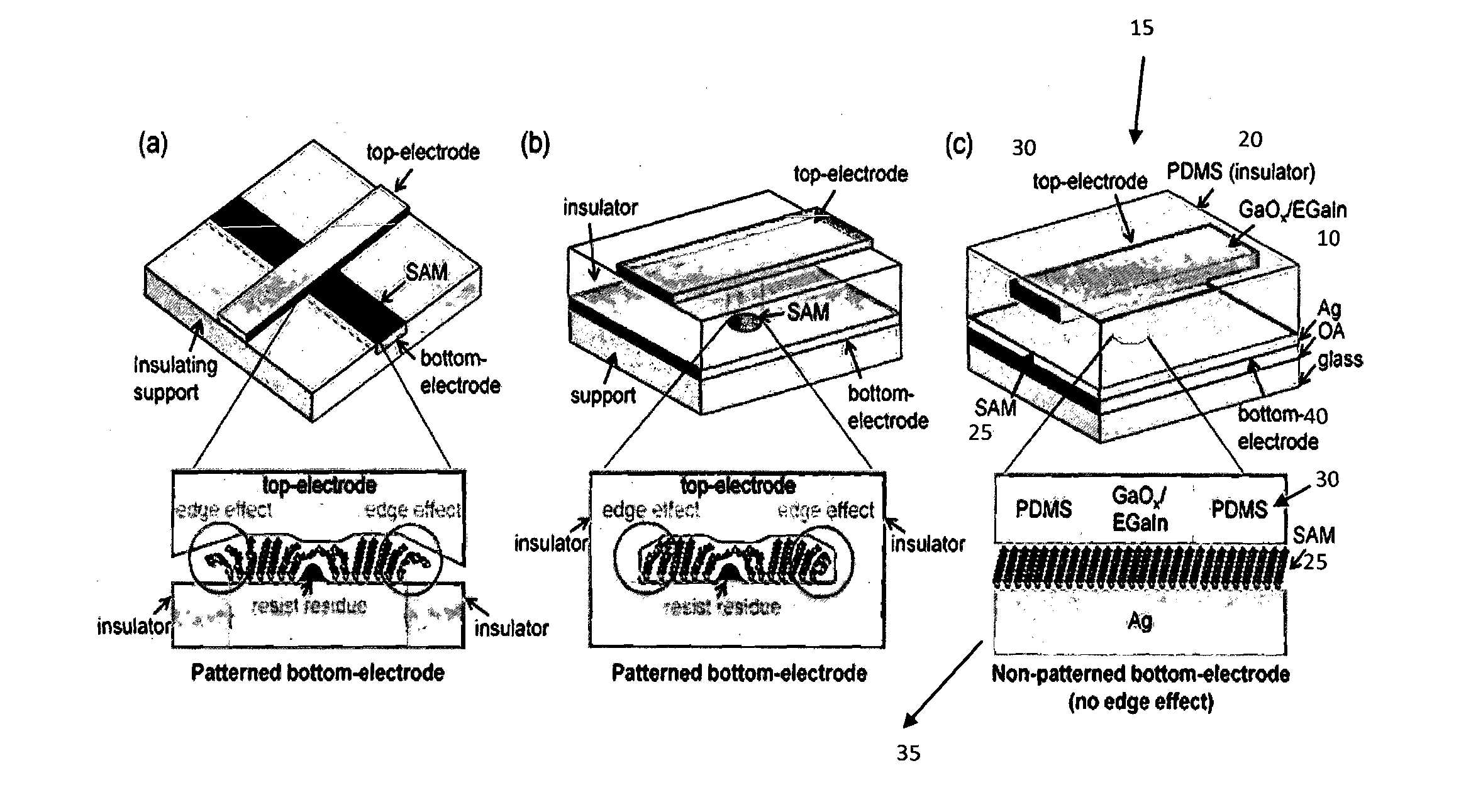
[0081]Junctions with GaOx / EGaIn Top-Electrodes

[0082]The EGaIn spontaneously forms a self-limiting layer of GaOx in air with a thickness of 0.7 nm and because of its non-Newtonian properties this material can be shaped. Therefore, unlike Hg, GaOx / EGaIn forms stable structures in PDMS micro-channels. The oxide layer also prevents the bulk EGaIn from alloying with the gold or silver bottom electrode which adds stability to junctions. The oxide layer is defective and contains oxygen vacancies, and it is highly conductive.

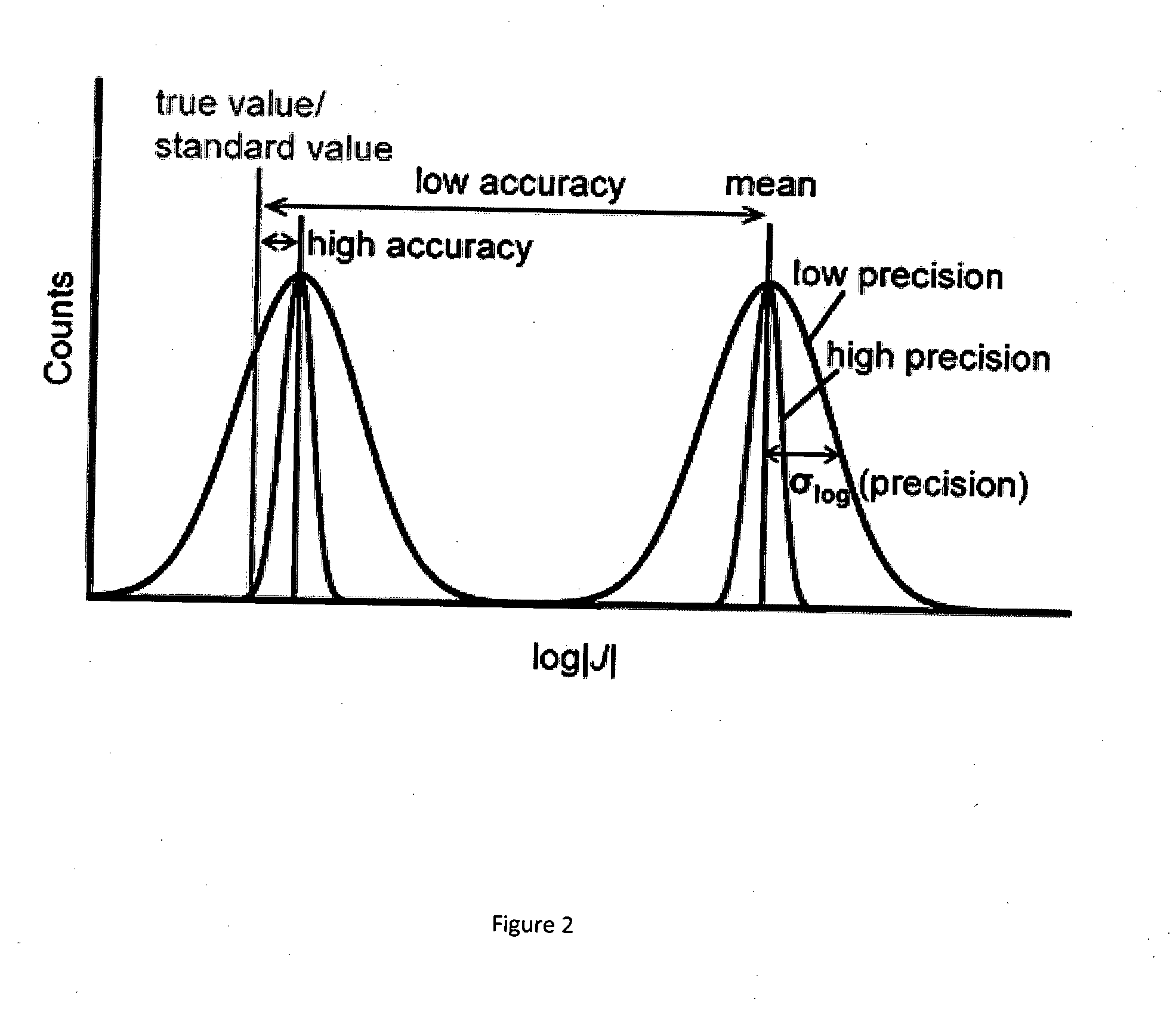
[0083]The precision of the data, that is, the width of the distributions of the values of J (see FIG. 2 for definitions), generated using junctions formed with cone-shaped tips of GaOx / EGaIn relies on the operator because the formation of the tips and bringing the tip in contact with the SAMs are usually performed with a manually operated manipulator. (Alternatively, piezo-controlled manipulators may be used.) For instance, the contact size, tip roughness, and the speed...


PUM

PropertyMeasurementUnit
Thicknessaaaaaaaaaa
Thicknessaaaaaaaaaa
Diameteraaaaaaaaaa

Abstract

The present invention relates to an electrical contact. In particular, it relates to an electrical contact capable of establishing an electrical contact with a soft material. More particular, the electrical contact comprises (a) a non-Newtonian liquid metal alloy, the non-Newtonian liquid metal alloy is formed in a polymer insulator, wherein the contact surface of the electrical contact that contacts the soft material is a smooth flat non-patterned surface, the surface comprising the non-Newtonian liquid metal alloy sandwiched between the polymer insulator. The microfluidic device comprising the electrical contact and a method for forming the electrical contact are also disclosed.

Description

FIELD OF THE INVENTION[0001]The present invention relates to an electrical contact. In particular, it relates to an electrical contact capable of establishing an electrical contact with a soft material.BACKGROUND OF THE INVENTION[0002]Many materials based on molecules, biomolecules, polymers, gels, living tissue, etc are so-called soft materials. Such soft materials have found its way into electronic devices known as molecular electronic devices. Commercial applications of such molecular electronic devices are in the form of thin-films in displays, organic light emitting diodes, or bendable devices. Despite these applications, many questions regarding the details of the mechanisms of charge transport across molecules and the molecule-electrode interfaces remain unanswered. Molecular electronic devices that are based on single molecules, or self-assembled monolayers (SAMs), are potentially good test-beds to study charge transport across molecules and the molecule-electrode interfaces...

Claims


Application Information

Patent Timeline
IPC IPC(8): H01L29/45B32B15/04H01L51/10
CPCH01L29/45H01L51/105B32B2307/202B32B2307/412B32B15/04B01L3/502707B01L3/502715B01L2300/0645B01L2300/0816B01L2400/0415G01N27/44791B81C1/00095B81B2201/058B81B2207/07H10K10/84
Inventor NIJHUIS, CHRISTIAN ALBERTUSWAN, ALBERTJIANG, LICHANDRAMATHI SUKUMARAN, SUCHAND SANGEETH
Owner NAT UNIV OF SINGAPORE
Why Eureka
Try Eureka