System and Method for Planarizing a Substrate

a substrate and system technology, applied in the field of microfabrication, can solve the problems of inability to use cmp for many process steps of microfabricating an integrated circuit, limited use of cmp, and high physical abrasion resistance of cmp, so as to achieve high controllability and accuracy

Active Publication Date: 2016-10-13
TOKYO ELECTRON LTD
View PDF2 Cites 11 Cited by
  • Summary
  • Abstract
  • Description
  • Claims
  • Application Information

AI Technical Summary

Benefits of technology

[0008]Introducing a photo acid generator and using projected light patterns to release photo acid as disclosed herein provides a highly controllable and accurate method to adjust z-height on a substrate, which can include using a laser galvanometer or digital light projection (DLP) chip providing light dose variation across a substrate. The result is a non-abrasive planarization process that can be finely controlled both spatially (across the wafer) and vertically (amount of material removed). These methods can provide selective planarization per die and selective planarization within each die. Such techniques can be executed using multiple tools, or within a single tool system, such as a coater / developer tool (also known as a track tool) commonly used for microfabrication. Planarization techniques herein can also be used for stacked die parts, including die or die-to-wafer configurations, and can planarize even with high topography and sharp edges of die configurations.

Problems solved by technology

Although chemical mechanical polishing can provide a planar surface on a wafer, there are limitations and drawbacks to using CMP.
Thus, CMP is a very harsh and physically abrasive process compared to other microfabrication techniques.
CMP, therefore, cannot be used for many process steps of microfabricating an integrated circuit.
For example, CMP cannot be used for microfabricating transistors and other front-end-of-line structures—especially when a gate oxide is exposed.
Moreover, CMP processes are very expensive to run, challenging to perform, and typically reduce yield of functional integrated circuits.

Method used


Image

  • System and Method for Planarizing a Substrate
  • System and Method for Planarizing a Substrate
  • System and Method for Planarizing a Substrate

Examples


Embodiment Construction

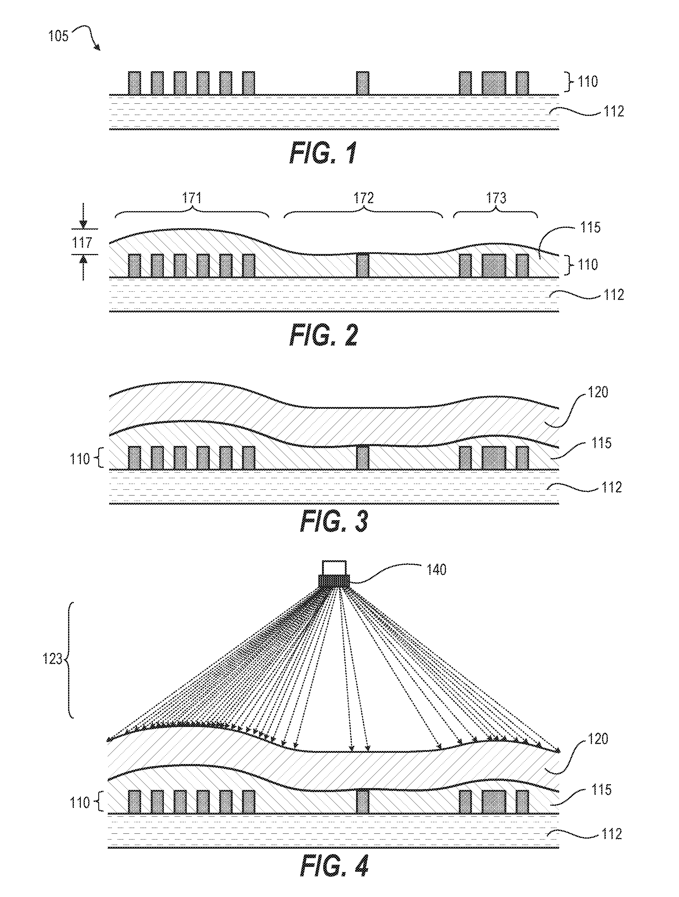
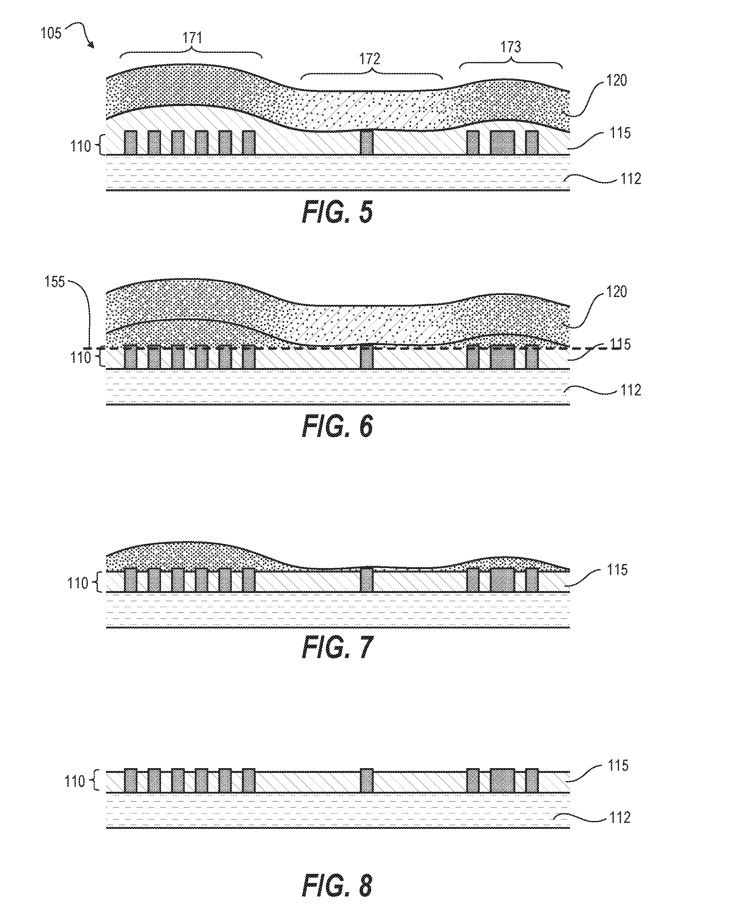
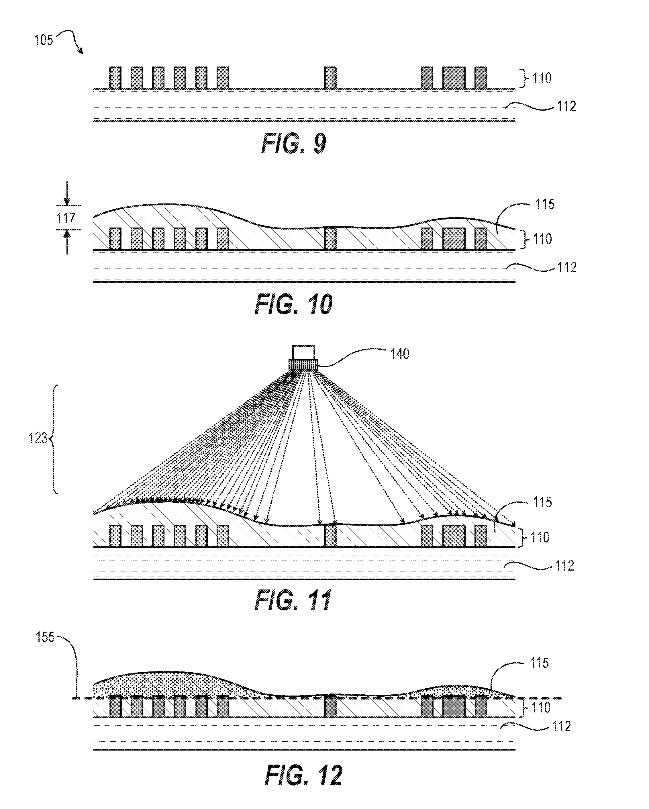
[0027]Techniques disclosed herein provide a chemical-based planarization process without mechanical polishing. Techniques include providing selective or differential planarization such that different regions of a substrate can have different amounts of material removed. In general, methods herein use photo-reactive generator compounds to generate solubility-changing agents. A specific pattern of light is projected onto a substrate containing such photo-reactive generator compounds to create different concentrations of solubility-changing agent(s) at specific locations across a substrate. These concentration differences then control an amount (height or depth) of material removed from a given film or layer at each specific location.

[0028]There are several embodiments encompassed by techniques herein. FIGS. 1-8 illustrate one example embodiment for planarizing a substrate. Referring now to FIG. 1, a substrate 105 is received having micro-fabricated structures 110 formed thereon. Note ...


PUM


Abstract

Techniques include providing selective or differential planarization such that different regions of a substrate can have different amounts of material removed. In general, methods herein use photo-reactive generator compounds to generate solubility-changing agents. A specific pattern of light is projected onto a substrate containing such photo-reactive generator compounds to create different concentrations of solubility-changing agent(s) at specific locations across a substrate. As generated solubility-changing agents are diffused into an underlying layer, these concentration differences then control an amount (height or depth) of material removed from a given film or layer at specific spatial locations on the substrate.

Description

CROSS REFERENCE TO RELATED APPLICATIONS[0001]The present application claims the benefit of U.S. Provisional Patent Application No. 62 / 146,480, filed on Apr. 13, 2015, entitled “System and Method for Planarizing a Substrate,” which is incorporated herein by reference in its entirety.BACKGROUND OF THE INVENTION[0002]This disclosure relates to microfabrication including microfabrication of integrated circuits.[0003]Semiconductor manufacturing includes photolithographic and patterning processes. Some photolithographic processes include coating a wafer with a thin film of bottom anti-reflective coating (BARC) material, followed by coating with a resist, and then exposing the wafer to a pattern of light as one of many process steps for creating microchips. Photolithographic and patterning processes typically benefit from a planar surface for depositing the various films and resists used to pattern and expose a wafer. Films can be specified to have a particular height and be planarized to ...

Claims


Application Information

Patent Timeline
Patent Type & Authority Applications(United States)
IPC IPC(8): H01L21/3105G03F7/32G03F7/20
CPCH01L21/31051G03F7/32G03F7/20G03F7/09G03F7/18G03F7/2057G03F7/30G03F7/70291H01L21/0273H01L21/31058G03F7/40G03F7/0035
Inventor DEVILLIERS, ANTON J.
Owner TOKYO ELECTRON LTD
Why Eureka
Try Eureka