Lead-Free Solder Alloy and Semiconductor Device

a technology of lead-free solder alloy and semiconductor device, which is applied in the direction of welding/cutting media/materials, manufacturing tools, and soldering apparatus, etc., can solve the problems of lead which is pointed out to be hazardous to human bodies, and achieve the effect of improving the reliability of the connection of the lead-free solder alloy and the semiconductor device in a high-temperature environmen

Inactive Publication Date: 2016-10-13
HITACHI LTD
View PDF5 Cites 5 Cited by
  • Summary
  • Abstract
  • Description
  • Claims
  • Application Information

AI Technical Summary

Benefits of technology

[0020]The effects obtained by typical aspects of the present invention will be briefly described below.
[0021]The connection reliability of solder connection between the lead-free solder alloy and the semiconductor device in a high-temperature environment can be improved.BRIEF DESCRIPTIONS OF THE DRAWINGS
[0022]FIG. 1 is a partial cross-sectional view showing an example of a structure of a principal part of a semiconductor device of an embodiment of the present invention;
[0023]FIG. 2 is a partial cross-sectional view showing an example of structures obtained before and after connection of a solder connection part of the semiconductor device shown in FIG. 1;
[0024]FIG. 3 is an enlarged partial cross-sectional view showing a structure of a part “A” of the semiconductor device shown in FIG. 1;
[0025]FIG. 4 is a plan view showing an example of a horizontal-direction structure of a solder alloy layer shown in FIG. 1;

Problems solved by technology

However, in recent years, as environmental consciousness increases, regulations for the lead which is pointed out to be hazardous to human bodies have started.

Method used


Image

  • Lead-Free Solder Alloy and Semiconductor Device
  • Lead-Free Solder Alloy and Semiconductor Device
  • Lead-Free Solder Alloy and Semiconductor Device

Examples


Embodiment Construction

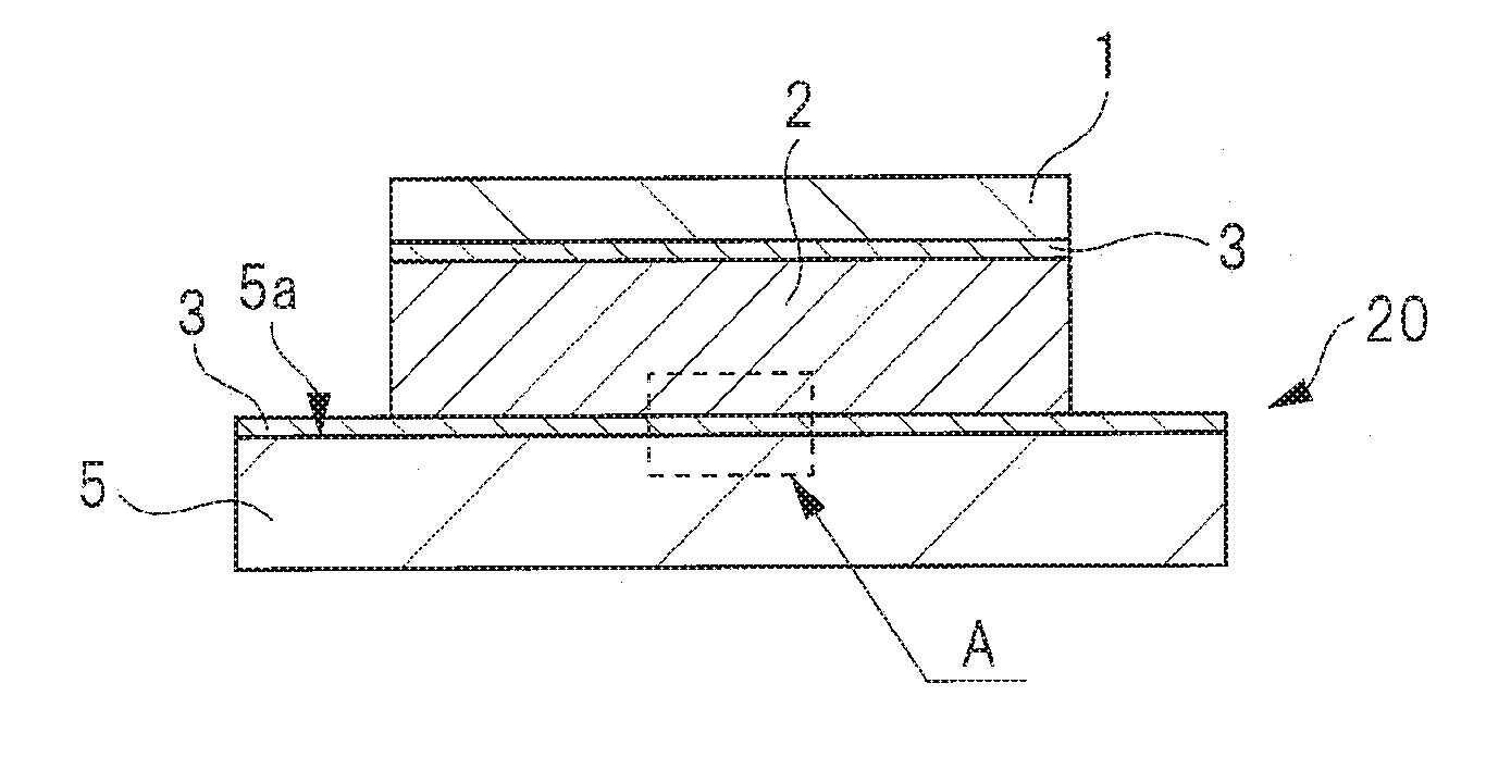
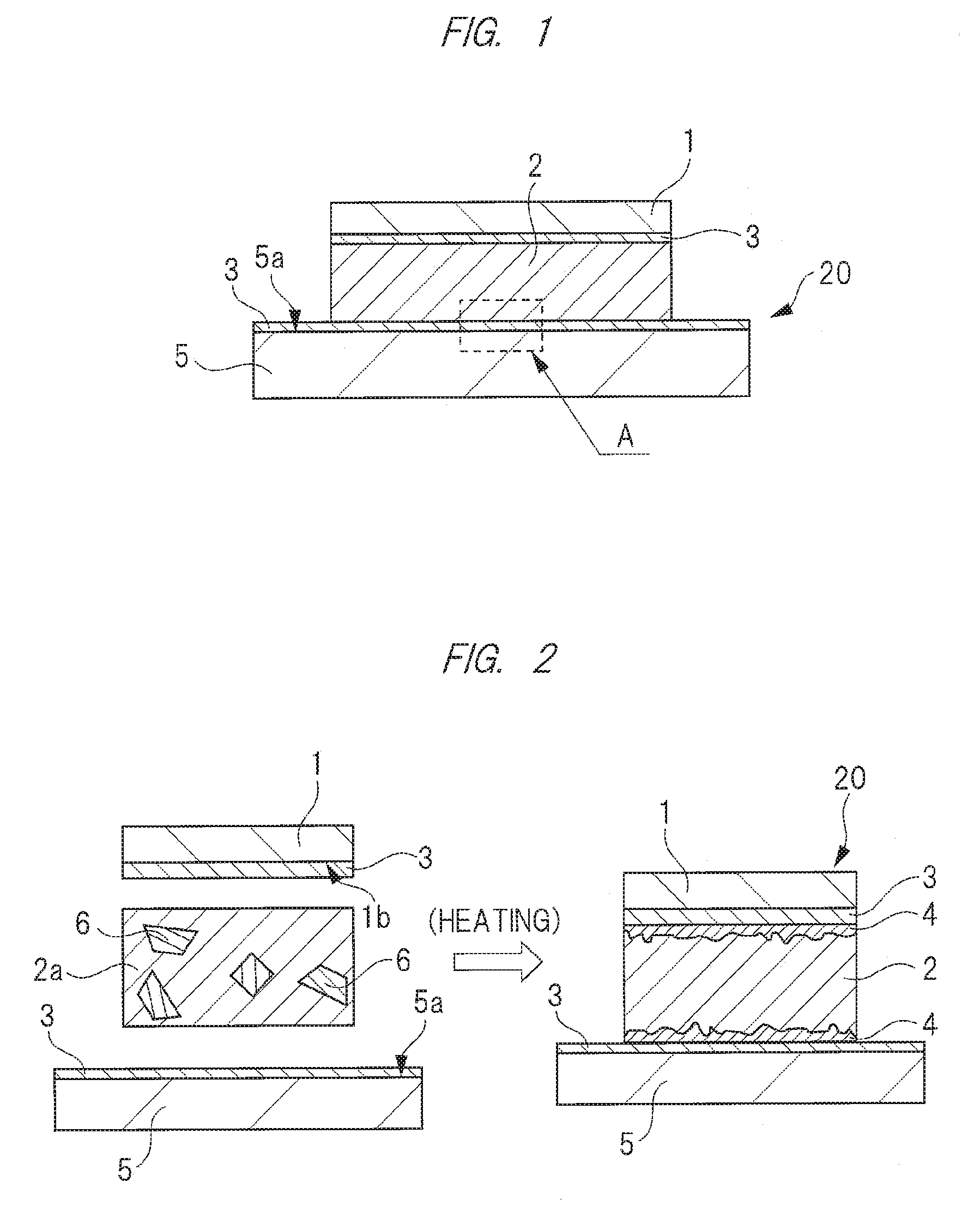
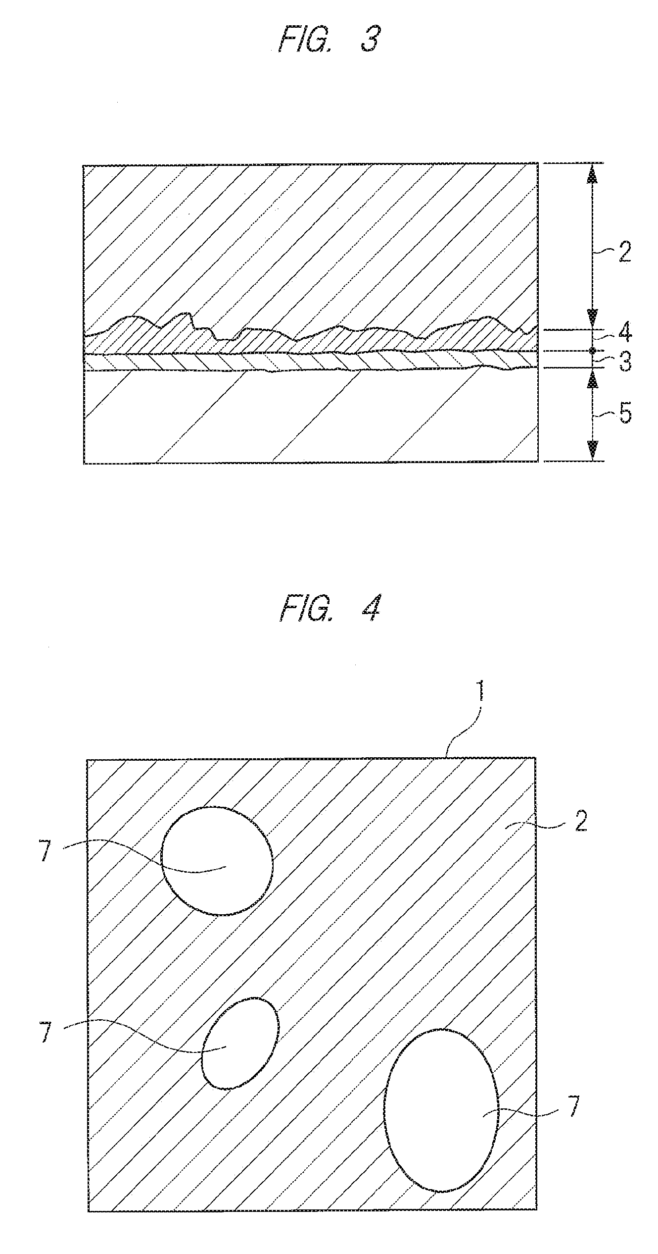
[0036]In the following embodiments, the description of the same or similar components are not repeated in principle unless otherwise required.

[0037]In the embodiments described below, the invention will be described in a plurality of sections or embodiments when required as a matter of convenience. However, these sections or embodiments are not irrelevant to each other unless otherwise stated, and the one relates to the entire or a part of the other as a modification example, details, or a supplementary explanation thereof.

[0038]Also, in the embodiments described below, when referring to the number of elements (including number of pieces, values, amount, range, and the like), the number of the elements is not limited to a specific number unless otherwise stated or except the case where the number is apparently limited to a specific number in principle. The number larger or smaller than the specified number is also applicable.

[0039]Further, in the embodiments described below, it goes...


PUM

PropertyMeasurementUnit
temperatureaaaaaaaaaa
solidus temperatureaaaaaaaaaa

Abstract

A semiconductor device 20 has: a semiconductor chip 1; a connected member 5 connected to the semiconductor chip 1 via a solder alloy (lead-free solder alloy) 2; and an external terminal electrically connected to the semiconductor chip 1. The above-described solder alloy 2 of the semiconductor device 20 is composed of: Cu of 5 to 10 weight %; any one, two, or more of Bi of 1 weight % or more and 4 weight % or less, Sb of 1 weight % or more and less than 10 weight %, and In of 1 weight % or more and 4 weight % or less; and Sn as a residual.

Description

TECHNICAL FIELD[0001]The present invention relates to a lead-free solder alloy and a semiconductor device, and, more particularly, the present invention relates to a lead-free solder alloy that is used under a high-temperature environment and a semiconductor device using the same.BACKGROUND ART[0002]Lead is generally contained in the solder serving as the connection member used in electric connection of the components of electric / electronic devices. However, in recent years, as environmental consciousness increases, regulations for the lead which is pointed out to be hazardous to human bodies have started.[0003]In Europe, the ELV Directive (End-of Life Vehicles directive, directive about a discarded automobile) which limits usage of the lead in an automobile and the RoHS (Restriction of the use of certain Hazardous Substances in electrical and electronic equipment) directive which prohibits usage of the lead in electric / electronic devices have been enforced.[0004]In the past, lead (...

Claims


Application Information

Patent Timeline
Patent Type & Authority Applications(United States)
IPC IPC(8): H01L23/00B23K35/26B23K35/02C22C13/00
CPCH01L24/29H01L2224/29564B23K35/262B23K35/0233H01L2924/01029H01L2924/01083H01L2924/01051H01L2924/01049H01L2924/0105H01L2924/014H01L2924/15787H01L2924/1203H01L2924/3512H01L2224/29655C22C13/00H01L24/83H01L2224/48095H01L2224/73265H01L2224/83101B23K35/26C22C13/02H01L23/40B23K35/0222B23K35/0227B23K35/0238H01L23/3735H01L2224/45144H01L2224/45147H05K3/3457H01L24/45H01L2224/32225H01L2924/00014H01L2924/00H01L2224/48227H01L2924/00012
Inventor MIYAZAKI, TAKAAKIIKEDA, OSAMU
Owner HITACHI LTD
Why Eureka
Try Eureka