Casing. esp. for semiconductor device, foot of such semiconductor device and mfg. method of such foot

A technology for semiconductors and shells, applied in the field of semiconductor devices and manufacturing feet, which can solve problems such as decomposition and tearing, large mechanical tension, etc.

Inactive Publication Date: 2004-08-11
INFINEON TECH AG
View PDF0 Cites 0 Cited by
  • Summary
  • Abstract
  • Description
  • Claims
  • Application Information

AI Technical Summary

Problems solved by technology

[0010] These mechanical tensions may be too great to disintegrate or tear the solder connection between a connector pin and the corresponding module or board pad

Method used


Image

  • Casing. esp. for semiconductor device, foot of such semiconductor device and mfg. method of such foot
  • Casing. esp. for semiconductor device, foot of such semiconductor device and mfg. method of such foot
  • Casing. esp. for semiconductor device, foot of such semiconductor device and mfg. method of such foot

Examples


Embodiment Construction

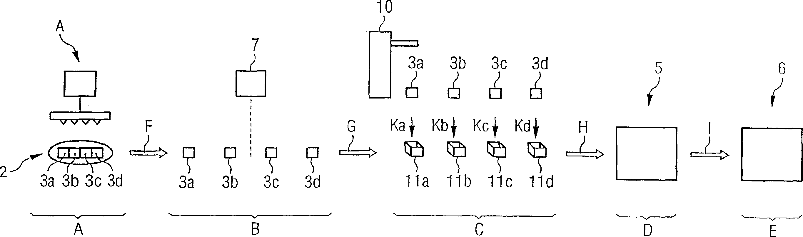
[0035] figure 1 Stations A, B, C, D through which some (absent a plurality of remaining stations, not shown) corresponding semiconductor devices 3a, 3b, 3c, 3d pass are schematically shown during manufacture of the semiconductor devices 3a, 3b, 3c, 3d.

[0036] At station A, semiconductor devices 3 a , 3 b , 3 c , 3 d are still available on a silicon disk or on a wafer 2 , respectively, subjected to one or a plurality of test methods by means of a test system 1 .

[0037] Prior to this, wafer 2 has, at a station not shown here and at figure 1 The previous stations A, B, C, D shown are subjected to the appropriate, conventional coating, exposure, etching, diffusion and implant processing steps.

[0038] The semiconductor devices 3a, 3b, 3c, 3d may, for example, be suitably integrated (analog or digital) electronic computing circuits, or semiconductor memory devices such as functional memory devices (PLAs, PALs, etc.) or desktop Type memory devices (such as ROMs or RAMs), such...


PUM


Abstract

The method involves one or more stamping process steps in which at least one pin is stamped out of a base body, especially a lead frame. The pin or a section of the pin is coated with a separate metal coating only after final stamping out of the pin. The end face of the outer end section of the pin is also coated with the metal coating. Independent claims are also included for the following: (a) a housing, especially for semiconducting components (b) and a semiconducting component pin.

Description

technical field [0001] The present invention relates to a casing, especially for a semiconductor device, a foot of the semiconductor device, and a method for manufacturing the foot. Background technique [0002] For the manufacture of semiconductor devices (such as corresponding, integrated (analog or digital) electronic computing circuits, semiconductor memory devices such as functional memory devices (PLAs, PALs, etc.) and desktop memory devices (such as ROMs or RAMs, especially are SRAMs and DRAMs)), so-called wafers (ie thin disks of single-crystal silicon) are used. [0003] The wafer is suitably processed (e.g., through a plurality of coating, exposure, etching, diffusion, and implant processing steps, etc.), and then, e.g., sawn (or, e.g., scraped and cut), so that individual devices can then be effect. [0004] After sawing the wafer, the devices - which can then function individually - are individually loaded into special housings or packages, respectively (eg cor...

Claims


Application Information

Patent Timeline
Patent Type & Authority Applications(China)
IPC IPC(8): H01L23/495H05K3/34
CPCH01L2924/0002H05K2201/10909H05K3/3426H01L23/49582H05K2201/10689Y02P70/50H01L2924/00
Inventor C·斯托肯M·多布勒G·埃格斯
Owner INFINEON TECH AG
Why Eureka
Try Eureka