

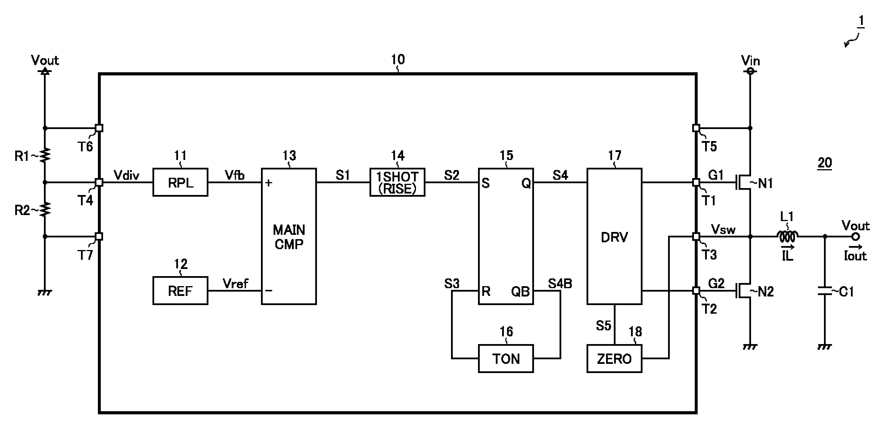
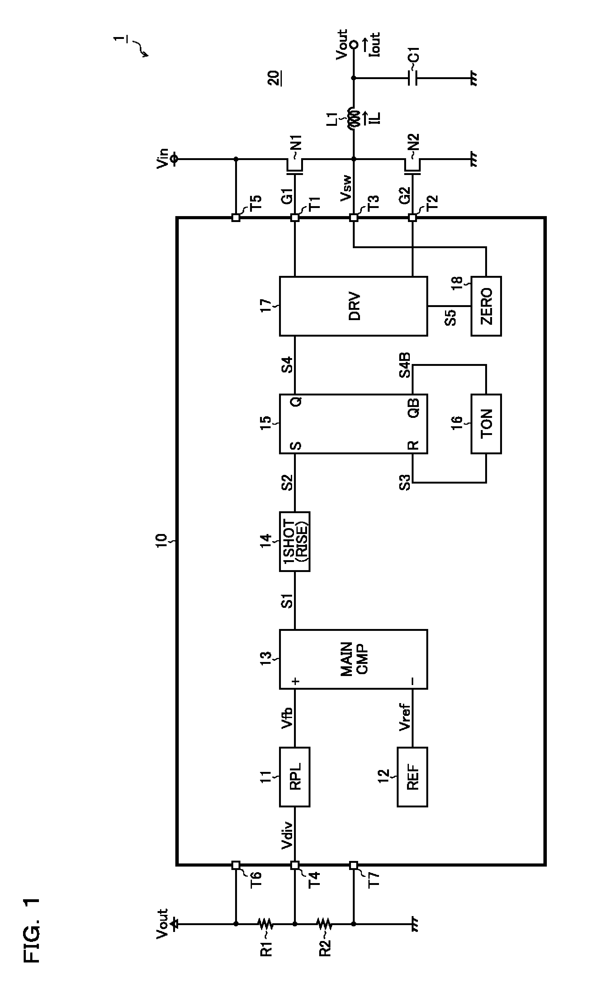
On-period setting circuit, power control ic, and switching power supply device
a technology of switching power supply and period setting circuit, which is applied in the direction of electric variable regulation, process and machine control, instruments, etc., can solve the problems of increased output ripple and discontinuous current mode, and achieve the effect of reducing output rippl
- Summary
- Abstract
- Description
- Claims
- Application Information
AI Technical Summary
Benefits of technology
Problems solved by technology
Method used
Image

Examples
first modified example
[0093]FIG. 8 is a circuit diagram showing a first modified example of the second voltage generator Y. The second voltage generator Y in this modified example is based on the basic configuration (FIG. 6) described previously, and further includes capacitors Y6 and Y7, P-channel MOS field-effect transistors Y8 to Y10, N-channel MOS field-effect transistors Y11 to Y14, and an inverter Y15. Accordingly, such circuit elements as find their counterparts in the basic configuration described previously are identified by the same reference signs as in FIG. 6, and no overlapping description will be repeated. The following description thus focuses on distinctive features of the first modified example.
[0094]A first end of the capacitor Y6 (with a capacitance value Cf1) is connected to an input terminal of the output voltage Vout. A second end of the capacitor Y6 is connected to the first end of the capacitor Y4.
[0095]The second end of the resistor Y2 and the second end of the capacitor Y4 are n...
second modified example
[0113]FIG. 9 is a circuit diagram showing a second modified example of the second voltage generator Y. The second voltage generator Y in this modified example is based on the first modified example (FIG. 8) described previously, and further includes, as additional circuit elements constituting a pull-up circuit, a resistor Y18, capacitors Y16 and Y17, and an N-channel MOS field-effect transistor Y19. Accordingly, such circuit elements as find their counterparts in the first modified example described previously are identified by the same reference signs as in FIG. 8, and no overlapping description will be repeated. The following description thus focuses on distinctive features of the second modified example.
[0114]A first end of the capacitor Y16 (with a capacitance value Ch1) is connected to the first end of the capacitor Y7. A second end of the capacitor Y16 and a first end of the resistor Y18 (with a resistance value Rh2) are both connected to the output terminal of the second vol...
third modified example
[0130]FIG. 11 is a circuit diagram showing a third modified example of the second voltage generator Y. The second voltage generator Y in this modified example is based on the second modified example (FIG. 9) described previously, and further includes a capacitor Y20, a P-channel MOS field-effect transistor Y21, and an N-channel MOS field-effect transistor Y22. Accordingly, such circuit elements as find their counterparts in the second modified example described previously are identified by the same reference signs as in FIG. 9, and no overlapping description will be repeated. The following description thus focuses on distinctive features of the third modified example.
[0131]A source of the transistor Y21 is connected to the output terminal of the second voltage VY. A drain of the transistor Y21 is connected to a first end of the capacitor Y20 (with a capacitance value Ch3) and to a drain of the transistor Y22. A second end of the capacitor Y20 and a source of the transistor Y22 are b...
PUM
 Abstract
Description
Claims
Application Information