Bus controller
Active Publication Date: 2016-10-20
ROHM CO LTD
13 Cites 50 Cited by
AI-Extracted Technical Summary
Problems solved by technology
Furthermore, this reduces power consumption ...
Benefits of technology
[0011]The present invention has been made in order to solve such a problem. Accordingly, it is an exemplary purpo...
Abstract
A power supply apparatus is provided, that supplies a bus voltage VBUS to a detachable device. A DC/DC converter generates a DC voltage VOUT used as the bus voltage VBUS. A USB controller receives the DC voltage VOUT as a power supply voltage, and detects whether or not the device is connected. The DC/DC converter generates the DC voltage VOUT such that (i) when the device is detected, the DC voltage VOUT has a specified voltage level, and such that (ii) when the device is not detected, the DC voltage VOUT has a voltage level that is lower than the specified voltage level and that is higher than a minimum operating voltage level required to operate the USB controller.
Application Domain
Batteries circuit arrangementsAc-dc conversion without reversal +3
Technology Topic
Dc converterUSB +4
Image
Examples
- Experimental program(1)
Example
[0045]The invention will now be described based on preferred embodiments which do not intend to limit the scope of the present invention but exemplify the invention. All of the features and the combinations thereof described in the embodiment are not necessarily essential to the invention.
[0046]In the present specification, the state represented by the phrase “the member A is connected to the member B” includes a state in which the member A is indirectly connected to the member B via another member that does not affect the electric connection therebetween, in addition to a state in which the member A is physically and directly connected to the member B.
[0047]Similarly, the state represented by the phrase “the member C is provided between the member A and the member B” includes a state in which the member A is indirectly connected to the member C, or the member B is indirectly connected to the member C via another member that does not affect the electric connection therebetween, in addition to a state in which the member A is directly connected to the member C, or the member B is directly connected to the member C.
[0048]FIG. 1 is a block diagram showing a power supply adapter 100 including a USB (Universal Serial Bus) controller 300 according to an embodiment. The power supply adapter 100 conforms (i.e. compliant or compatible) to the USB standard. The power supply adapter 100 supplies a bus voltage VBUS to a device 500 configured as a load that is detachably connected to the power supply adapter 100.
[0049]In the present embodiment, the power supply adapter 100 is configured as an AC adapter that receives an AC voltage VAC so as to generate the bus voltage VBUS. The power supply adapter 100 is configured as an AC/DC converter including an input rectifier circuit 102, a smoothing capacitor 104, and a power supply apparatus 200. The input rectifier circuit 102 rectifies the AC voltage VAC. For example, the input rectifier circuit 102 may be configured as a diode bridge circuit that full-wave rectifies the AC voltage VAC. The smoothing capacitor 104 is connected to the output of the input rectifier circuit 102, so as to smooth the output voltage of the input rectifier circuit 102.
[0050]The power supply apparatus 200 receives the output voltage of the input rectifier circuit 102 as an input voltage VIN, and steps down the input voltage VIN so as to convert the input voltage VIN into a DC output voltage VOUT. The output voltage VOUT is supplied to the device 500 as a bus voltage VBUS.
[0051]The power supply apparatus 200 includes a DC/DC converter 202, an output switch 204, and a USB controller 300. The power supply adapter 100 includes a connector 206. The connector 206 is configured as a receptacle or otherwise a plug. The connector 206 is directly connected to the device 500 or otherwise is connected to the device 500 via a USB cable. The DC/DC converter 202 receives the output voltage VIN of the input rectifier circuit 102, so as to generate the DC voltage VOUT that is to be used as the bus voltage VBUS. The output switch 204 is arranged between an output 214 of the
[0052]DC/DC converter 202 and the connector 206.
[0053]A power supply (VDD) terminal of the USB controller 300 is connected to a node between the DC/DC converter 202 and the output switch 204. The USB controller 300 operates receiving the DC voltage VOUT as a power supply voltage. The USB controller 300 is configured to be capable of detecting at least the presence or absence of the device 500 configured as a load.
[0054](i) When the USB controller 300 has detected the device 500, the DC/DC converter 202 generates the DC voltage VOUT having a specified level. On the other hand, (ii) when the USB controller 300 has detected no device 500, the DC/DC converter 202 generates the DC voltage VOUT having a standby voltage level V0 that is determined so as to be lower than the specified voltage level. The standby voltage level V0 is determined so as to be higher than a minimum operating voltage VMIN designed for the USB controller 300. Specifically, the standby voltage level V0 may be set so as to be slightly higher than the minimum operating voltage VMIN. For example, the standby voltage level V0 may be set to be several hundreds of mV higher than the minimum operating voltage VMIN. As an example, the USB controller 300 is designed to have a minimum operating voltage VMIN of 3.1 V and a standby voltage level V0 of 3.3 V. The minimum operating voltage VMIN is determined depending on the manufacturing process for the USB controller 300. With a manufacturing process that will be developed in the future, the USB controller 300 has the potential to have a further reduced minimum operating voltage VMIN.
[0055]Furthermore, (i) when the USB controller 300 has detected the device 500, the USB controller 300 turns on the output switch 204. On the other hand, (ii) when the USB controller 300 has detected no device 500, the USB controller 300 turns off the output switch 204. When the output switch 204 is turned on, the bus voltage VBUS having substantially the same value as the output voltage VOUT is output via the connector 206 (hot state). On the other hand, when the output switch 204 is turned off, the output voltage of the connector 206 becomes zero (cold state).
[0056]In the present embodiment, the USB controller 300 conforms to the USB-PD specification, and further conforms to the USB Type-C specification. The USB controller 300 is configured to select one from among multiple specified voltage levels (V1=5 V, V2=12 V, V3=20 V) according to negotiation with the device 500.
[0057]In the present embodiment, the DC/DC converter 202 is configured as an insulated DC/DC converter. A transformer T1 includes a primary winding W1 and a secondary winding W2. A secondary-side rectifier circuit 210 is connected to the secondary winding W2, and outputs the DC voltage VOUT. A switching transistor M1 is connected to the primary winding W1. A photocoupler 212 includes a light-emitting element 212a and a light-receiving element 212b.
[0058]A feedback circuit 220 includes a shunt regulator 222 and a voltage dividing circuit 224. The voltage dividing circuit 224 includes resistors R11 and R12. The voltage dividing circuit 224 divides the DC voltage VOUT so as to generate a detection voltage VOUTS. The shunt regulator 222 is arranged such that its cathode (K) is connected to the photocoupler 212, its anode (A) is grounded, and its input (REF) receives the detection voltage VOUTS from the voltage dividing circuit 224 as an input signal. Specifically, the shunt regulator 222 is connected to the light-emitting element 212a of the photocoupler 212 so as to drive the light-emitting element 212a with a current IERR that corresponds to the difference between the detection voltage VOUTS and a reference voltage VREF configured as the target value of the detection voltage VOUTS. It should be noted that the bias method and the phase compensation method for the photocoupler 212 are not restricted in particular. Rather, known techniques may preferably be employed.
[0059]The primary-side controller 230 switches on and off the switching transistor M1 according to a feedback signal VFB that corresponds to a current IFB that flows through the light-receiving element 212b of the photocoupler 212. The primary-side controller 230 may be configured using known techniques. That is to say, the control method and the circuit format of the primary-side controller 230 are not restricted in particular.
[0060]The output voltage VOUT of the DC/DC converter 202 is stabilized to the following voltage level by means of such a feedback control operation.
VOUT=VREF×(1+R11/R12) (1)
[0061]As described above, the output voltage VOUT of the DC/DC converter 202 is switched between the specified voltage levels (V1 through V3) and the standby voltage level (V0) according to the presence or absence of the device 500. Furthermore, such an arrangement is capable of switching the specified voltage level between the voltage levels V1 through V3 based on negotiation with the device 500. The USB controller 300 controls the feedback circuit 220 in order to switch the voltage level of the DC voltage VOUT. The feedback circuit 220 is configured to be capable of changing the current IERR according to the control operation of the USB controller 300.
[0062]FIGS. 2A and 2B are circuit diagrams each showing an example configuration of the feedback circuit 220. A feedback circuit 220a shown in FIG. 2A is capable of changing the reference voltage VREF, so as to switch the DC voltage VOUT between multiple voltage levels V0, V1, V2, and V3.
[0063]Specifically, the shunt regulator 222a includes a transistor M2, a reference voltage source 226, and an error amplifier 228. The transistor M2 is arranged between the cathode (K) terminal and the anode (A) terminal. The reference voltage source 226 is configured as a variable voltage source, and generates a variable reference voltage VREF according to a control signal CNT received from the USB controller 300. The output of the error amplifier 228 is connected to the control terminal (base) of the transistor M2. The error amplifier 228 amplifies the difference between the detection voltage VOUTS input to the REF terminal and the reference voltage VREF.
[0064]A feedback circuit 220b shown in FIG. 2B changes the value represented by the aforementioned Expression (1), i.e., (1 +R11/R12), so as to switch the DC voltage VOUT between the multiple voltage levels V0, V1, V2, and V3.
[0065]A voltage dividing circuit 224b shown in FIG. 2B is configured to be capable of changing the voltage division ratio represented by R12/(R11+R12). For example, the resistor R12 may be configured as a variable resistor having a resistance value that can be switched according to the control signal CNT received from the USB controller 300. Also, the resistor R11 may be configured as a variable resistor. The division ratio is configured as the reciprocal of Expression (1), i.e., the reciprocal of (1+R11/R12).
[0066]The above is the overall configuration of the power supply adapter 100. Next, description will be made regarding the USB controller 300.
[0067]FIG. 3 is a block diagram showing the USB controller 300. The USB controller 300 includes a power supply line 302, a detector 304, a feedback control unit 306, a switch control unit 308, and a communication unit 310, which are configured as a function IC (Integrated Circuit) integrated on a single semiconductor substrate.
[0068]The VDD terminal is connected to the output of the secondary-side rectifier circuit 210, and receives the DC voltage VOUT as a power supply voltage. The DC voltage VOUT is supplied to an internal circuit of the USB controller 300 via the power supply line 302.
[0069]The detector 304 detects the presence or absence of the device 500. With the USB Type-C specification, the detector 304 detects the presence or absence of the device 500 (attachment or detachment of a cable) based on the state of the pin CC1/CC2 (Configuration Channel).
[0070]The feedback control unit 306 refers to the detection result obtained by the detector 304. (i) When the device 500 has been detected, the feedback control unit 306 controls the feedback circuit 220 so as to generate the DC voltage VOUT having a voltage level selected from among the specified voltage levels V1 through V3. On the other hand, (ii) when the device 500 has not been detected, the feedback control unit 306 controls the feedback circuit 220 so as to generate the DC voltage VOUT having the standby voltage level V0. With a combination of the feedback control unit 306 and the feedback circuit 220a shown in FIG. 2A, the feedback control unit 306 controls the reference voltage VREF. With a combination of the feedback control unit 306 and the feedback circuit 220b shown in FIG. 2B, the feedback control unit 306 controls the voltage division ratio set for the voltage dividing circuit 224b.
[0071]The USB controller 300 that supports the USB-PD specification includes the communication unit 310 that provides communication with the device 500. The bus voltage VBUS to be supplied to the device 500 is selected from among the multiple specified voltage levels V1 through V3 according to communication (negotiation) between the communication unit 310 and the device 500. The feedback control unit 306 controls the feedback circuit 220 so as to supply the voltage thus selected.
[0072]The above is the basic configuration of the USB controller 300. Next, description will be made regarding the operation of the power supply apparatus 200.
[0073]The advantages of the power supply apparatus 200 can be clearly understood in comparison with the following comparison technique. Accordingly, description will be made below regarding such a comparison technique.
Comparison Technique
[0074]FIG. 4 is an operation waveform diagram showing the operation of a power supply apparatus according to a comparison technique. In the comparison technique, the standby voltage level V0 is not defined. FIG. 4 shows, in the following order beginning from the top, the presence or absence of connection of the device 500 (high level represents “connection”, and low level represents “disconnection”), the DC voltage VOUT, the state of the output switch 204, and the bus voltage VBUS.
[0075]In a state in which the device 500 has not been detected (device 500 disconnection state) before the time point t0, the output switch 204 is turned off. Accordingly, the bus voltage VBUS is set to zero, i.e., is set to the cold state, regardless of the voltage level set for the DC voltage VOUT.
[0076]Even in the cold state, the USB controller 300 is required to operate. Accordingly, even in this state, the DC voltage VOUT cannot be lowered to zero. With the comparison technique, when the device 500 is not connected, the DC voltage VOUT is set to the voltage level V1 having the lowest voltage level (lowest specified voltage level) from among the specified voltage levels V1 through V3.
[0077]At the time point t0, the device 500 is connected. During a period from the time point t0 up to the time point t1, negotiation is performed between the power supply apparatus and the device 500. During the negotiation, the bus voltage VBUS is set to V1. Subsequently, the bus voltage VBUS is selected from among the multiple specified voltage levels based on the negotiation result. In this example, V2=12 V is selected as the bus voltage VBUS. At the time point t1, the DC voltage VOUT is raised to 12 V, and the bus voltage VBUS follows the DC voltage VOUT thus raised. Subsequently, the output voltage VOUT of the DC/DC converter 202 is stabilized to V2=12 V. In this state, the output voltage VOUT of the DC/DC converter 202 is supplied to the device 500 as the bus voltage VBUS.
[0078]When the device 500 is detached at the time point t2, the output switch 204 is turned off, which switches the power supply apparatus to the cold state. Furthermore, the output voltage VOUT of the DC/DC converter 202 is lowered to the lowest specified voltage level V1.
[0079]The above is description of the comparison technique. Next, description will be made with reference to FIG. 5 regarding the operation of the power supply apparatus 200 according to the embodiment. FIG. 5 is an operation waveform diagram showing the operation of the power supply apparatus 200 according to the embodiment.
[0080]In a state in which the device 500 has not been detected (device 500 disconnection state) before the time point t0, the output switch 204 is turned off, which sets the bus voltage VBUS to zero. That is to say, the power supply apparatus 200 is set to the cold state. In the device 500 disconnection state, with the present embodiment, the DC voltage VOUT is maintained at the standby voltage level V0 (3.3 V) that is lower than the lowest specified voltage level V1.
[0081]When the device 500 has been detected at the time point t0, the DC voltage VOUT is switched from 3.3 V to 5 V. After the DC voltage VOUT is stabilized to 5 V, the USB controller 300 turns on the output switch 204. In this state, the bus voltage VBUS having a voltage level of 5 V is supplied to the device 500. Subsequently, the voltage level of the bus voltage VBUS is determined to be the specified voltage level V2 based on the negotiation result. At the time point t1, the voltage level of the DC voltage VOUT is switched to 12 V.
[0082]When the device 500 has been detached at the time point t2, the output switch 204 is turned off, which switches the power supply apparatus 200 to the cold state. Furthermore, the output voltage VOUT of the DC/DC converter 202 is lowered to the standby voltage level V0.
[0083]The above is the operation of the power supply apparatus 200 according to the embodiment.
[0084]With such a comparison technique, in the period between the time point t0 and the time point t1, the power consumption of the USB controller 300 is represented by V1×I1. In contrast, with the embodiment, such an arrangement is capable of providing reduced power consumption as represented by V0×I1. In a case in which V1=5 V and V0=3.3 V, such an arrangement is capable of providing the USB controller 300 with a reduction of 30% or more in power consumption in the standby state.
[0085]Furthermore, in the standby state, in addition to the USB controller 300, the feedback circuit 220 also consumes electric power. Specifically, the voltage dividing circuit 224 consumes electric power represented by VOUT2/(R1+R2). Thus, such an arrangement is capable of also providing the voltage dividing circuit 224 with a reduction of 30% or more in power consumption.
[0086]In addition, the photocoupler 212 and the shunt regulator 222 also consume electric power as represented by IERR×VOUT. Thus, such an arrangement is capable of also providing the photocoupler 212 and the shunt regulator 222 with a reduction of 30% or more in power consumption.
[0087]As described above, with the power supply apparatus 200 according to the embodiment, the standby voltage level V0 is determined such that it is lower than the minimum specified voltage level V1 defined in the USB standard. With such an arrangement, the DC/DC converter 202 is configured to be capable of generating the DC voltage VOUT having the standby voltage level V0. When the device 500 is not connected to the power supply apparatus 200, the output voltage VOUT of the DC/DC converter 202 is lowered to V0, thereby providing the USB controller 300 and the secondary side of the DC/DC converter 202 with a reduction in power consumption in the standby state.
[0088]FIG. 6 is a function block diagram showing the USB controller 300 that conforms to the USB-PD specification and the USB Type-C specification.
[0089]A control logic unit 320 integrally controls the overall operation of the USB controller 300. An interface circuit 330 functions as a physical layer (PHY) of a configuration channel (CC). A bus voltage detector 332 detects and monitors the bus voltage VBUS. A port detector 334 detects whether or not the device 500 is connected to the CC1/CC2 port (pin). Furthermore, with the USB Type-C specification, such an arrangement is capable of detecting the orientation of a reversible cable. A transceiver 336 includes a transmitter (BB-TX) and a receiver (BB-RX), and communicates with the device 500 via the configuration channel.
[0090]A switch driver 340 controls an on/off operation of the output switch 204 according to an instruction from the control logic unit 320. The switch driver 340 includes an unshown charge pump circuit.
[0091]A discharge circuit 342 is connected to the output of the secondary-side rectifier circuit 210. The discharge circuit 342 turns on according to an instruction from the control logic unit 320, which discharges the charge stored in an output capacitor C1 included in the secondary-side rectifier circuit 210. A voltage monitoring unit 344 monitors the output voltage VOUT of the secondary-side rectifier circuit 210. The monitoring result is input to the control logic unit 320.
[0092]The discharge circuit 346 is connected to the connector side of the output switch 204. The discharge circuit 346 turns on according to an instruction from the control logic unit 320, which discharges the charge stored on the connector side. A voltage monitoring unit 348 monitors the bus voltage VBUS. The monitoring result is input to the control logic unit 320.
[0093]A current detection circuit 350 detects a current supplied to the device 500 via the output switch 204. The detection result is input to the control logic unit 320.
[0094]Description will be made again with reference to FIG. 5 regarding the operation of the USB controller 300 shown in FIG. 6. The port detector 334 monitors the state of the CC port so as to detect whether or not the device 500 is connected. Furthermore, with the USB Type-C specification, the cable is configured as a reversible cable having a front/back symmetrical structure. When the cable is connected, the device 500 is connected to either the CC1 port or the CC2 port. The port detector 334 judges whether the device 500 is connected to the CC1 port or the CC2 port. It can be said that the port detector 334 corresponds to the detector 304 shown in FIG. 3.
[0095]Before the time point (time point 0) at which the port detector 334 has detected the device 500, the control logic unit 320 instructs the switch driver 340 to turn off the output switch 204. This sets the output to the cold state. It can be said that a part of the control logic unit 320 and the switch driver 340 correspond to the switch control unit 308 shown in FIG. 3.
[0096]Furthermore, in this state, the control logic unit 320 controls the feedback circuit 220 such that the output VOUT of the DC/DC converter 202 becomes V0. It can be said that a part of the control logic unit 320 corresponds to the feedback control unit 306 shown in FIG. 3.
[0097]At the time point t0, the port detector 334 detects the device 500. In this state, the control logic unit 320 controls the feedback circuit 220 such that the output VOUT of the DC/DC converter 202 becomes V1 (=5 V). Furthermore, the control logic unit 320 instructs the switch driver 340 to turn on the output switch 204. This establishes a Type-C connection.
[0098]After the Type-C connection has been established, negotiation is performed between the transceiver 336 and the device 500. In this step, the target level of the bus voltage VBUS is selected from among the specified voltage levels V1 through V3. In this example, the specified voltage level V2=12 V is selected. At the time point t1, the control logic unit 320 controls the feedback circuit 220 such that the output VOUT of the DC/DC converter 202 becomes V2 (=12 V). When the bus voltage VBUS reaches the specified voltage level V2 thus selected, the control logic unit 320 asserts a flag PS READY.
[0099]After the time point t1, the port detector 334 repeatedly monitors the device 500, and detects whether or not the cable or otherwise the device 500 is disconnected. When the device 500 has been disconnected at the time point t2, the control logic unit 320 lowers the output voltage VOUT to the standby voltage level V0. Furthermore, the control logic unit 320 turns off the output switch 204. The above is the operation of the USB controller 300 shown in FIG. 6.
[0100]FIGS. 7A and 7B are external views each showing the power supply adapter 100. A power supply adapter 100a shown in FIG. 7A is referred to as a “receptacle output type power supply adapter”. Such a power supply adapter 100a includes the connector 206 configured as a receptacle (female connector). With such a type of power supply adapter, when the device 500 is not connected, there is a need to set the output to the cold state.
[0101]A power supply adapter 100b shown in FIG. 7B is referred to as a “captive cable type power supply adapter” having a plug (cable) output configuration. With such a type of power supply adapter, it is recommended that the output be set to the cold state when the device 500 is disconnected. However, such a type of power supply adapter allows the output to be maintained in the hot state even when the device 500 is not connected. That is to say, with the power supply adapter 100b shown in FIG. 7B, the output switch 204 may be omitted.
[0102]Description has been made above regarding the present invention with reference to the embodiment. The above-described embodiment has been described for exemplary purposes only, and is by no means intended to be interpreted restrictively. Rather, it can be readily conceived by those skilled in this art that various modifications may be made by making various combinations of the aforementioned components or processes, which are also encompassed in the technical scope of the present invention. Description will be made below regarding such modifications.
First Modification
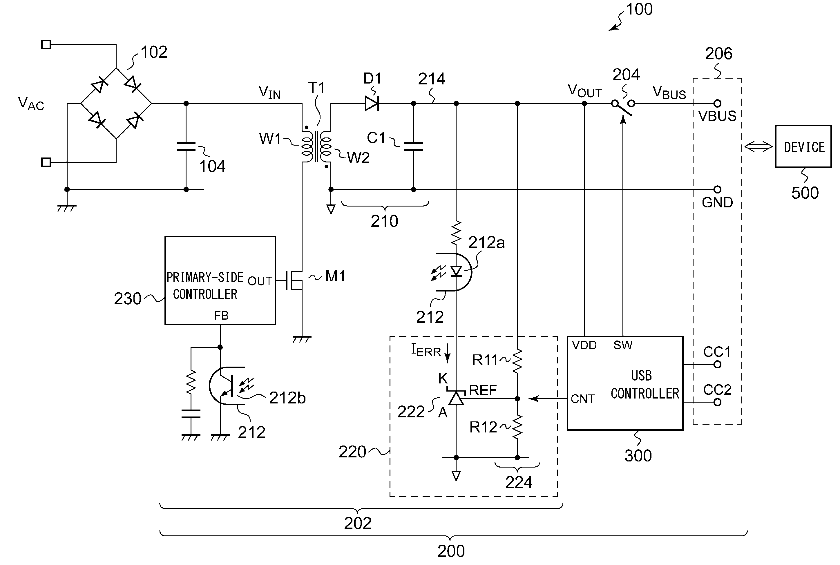
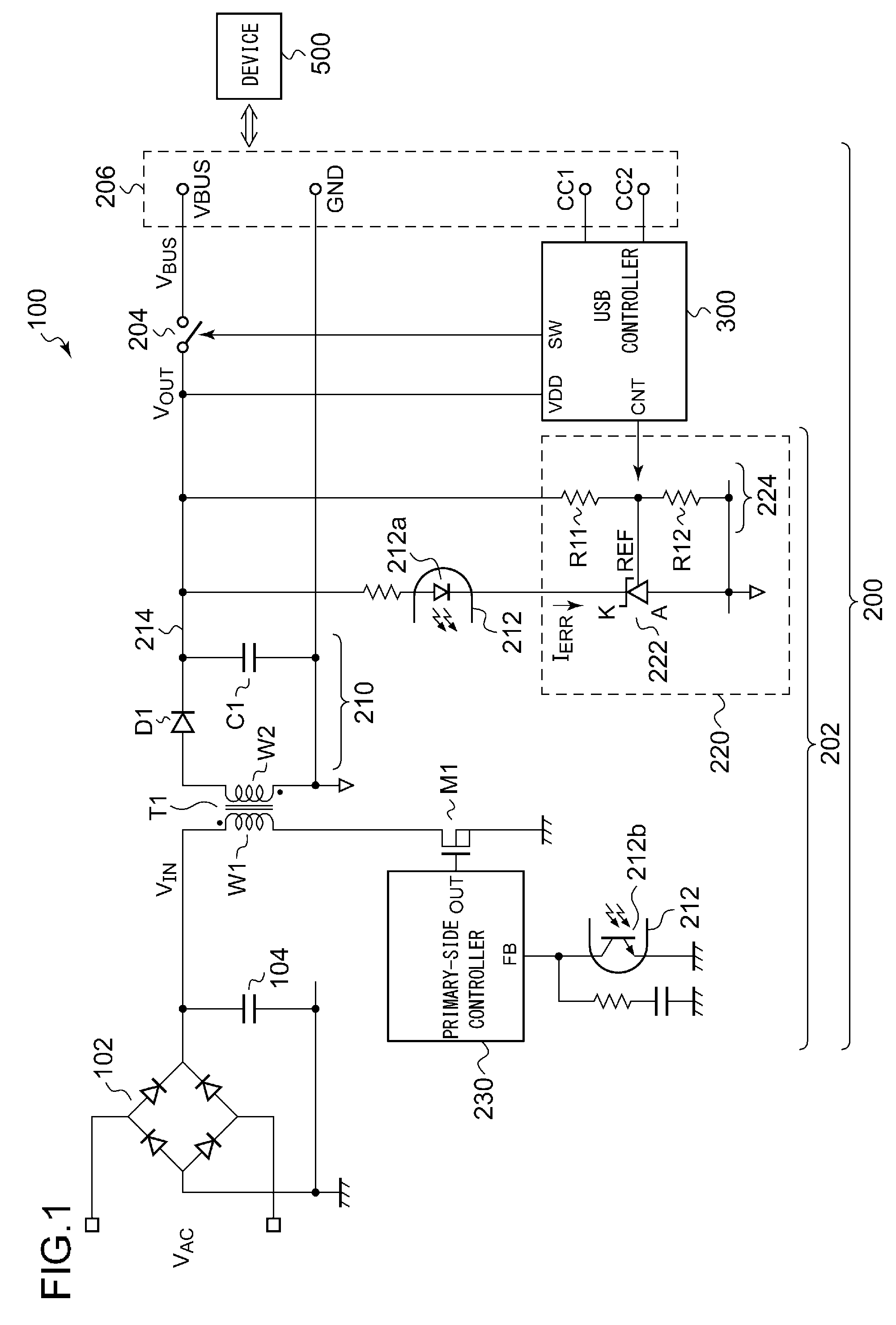
[0103]Description has been made in the embodiment regarding the USB controller 300 that supports both the USB-PD specification and the USB Type-C specification. However, the present invention is not restricted to such an arrangement.
[0104](i) For example, the present invention is also applicable to the USB controller 300 that supports only the USB Type-C specification. In this case, with such an arrangement, only V1=5 V is prepared as the specified voltage level. Also, the DC/DC converter 202 may preferably be configured to switch the DC voltage VOUT between two values, i.e., V0 and V1.
[0105](ii) Conversely, the present invention is also applicable to the USB controller 300 that supports only the USB-PD specification. In this case, a function for detecting the cable orientation or the like may be omitted.
Second Modification
[0106]Description has been made in the embodiment regarding the USB controller 300. However, the present invention is not restricted to such an arrangement. In addition to the present USB standard, the present invention is applicable to other USB standards which will be developed in the future, and voltage supply systems employing a similar architecture derived from the USB standard. Also, the kind of bus is not restricted to such a USB bus. Also, the present invention is applicable to other standards that differ from the USB standard, examples of which include the Quick Charge standard. The Quick Charge standard (Quick Charge 2.0) supports bus voltages VBUS of 5 V, 9 V, and 12 V.
Third Modification
[0107]Description has been made in the embodiment regarding the DC/DC converter 202 configured as a flyback converter. However, the topology of the DC/DC converter 202 is not restricted in particular. For example, the DC/DC converter 202 may be configured as a synchronous rectification DC/DC converter. Also, the DC/DC converter 202 may be configured as a forward converter. Also, the DC/DC converter 202 may be configured as a converter employing an inductor, instead of a converter employing the transformer T1.
Fourth Modification
[0108]The power supply adapter 100 is not restricted to such an AC power supply adapter as shown in FIGS. 7A and 7B. With the USB-PD specification, it is assumed that the power supply adapter 100 is mounted on various kinds of electronic devices such as TVs, computers, and the like, so as to support a bus voltage supply function. Thus, the power supply adapter 100 may be built into such an electronic device.
Fifth Modification
[0109]All of or a part of the feedback circuit 220 may be built into the USB controller 300.
[0110]While the preferred embodiments of the present invention have been described using specific terms, such description is for illustrative purposes only, and it is to be understood that changes and variations may be made without departing from the spirit or scope of the appended claims.
PUM


Description & Claims & Application Information
We can also present the details of the Description, Claims and Application information to help users get a comprehensive understanding of the technical details of the patent, such as background art, summary of invention, brief description of drawings, description of embodiments, and other original content. On the other hand, users can also determine the specific scope of protection of the technology through the list of claims; as well as understand the changes in the life cycle of the technology with the presentation of the patent timeline. Login to view more.
Similar technology patents
Efficient route update protocol for wireless sensor network
Owner:SAMSUNG ELECTRONICS CO LTD +1
Method and system of unmanned plane omnibearing obstacle avoidance based on binocular vision
Owner:SHENZHEN AUTEL INTELLIGENT AVIATION TECH CO LTD
Demand response method, computer-readable medium and system
Owner:SAMSUNG ELECTRONICS CO LTD
Systems and methods for selectively invoking positioning systems for mobile device control applications using accelerometer measurements
Owner:ILLUME SOFTWARE
Nonvolatile memory cell, storage device and nonvolatile logic circuit
Owner:SONY SEMICON SOLUTIONS CORP
Classification and recommendation of technical efficacy words
- reduce power consumption
Electrode array for use in medical stimulation and methods thereof
Owner:CASE WESTERN RESERVE UNIV
Method of placing and routing for power optimization and timing closure
Owner:GOLDEN GATE TECH
Method of reselecting a cell based on priorities
Owner:LG ELECTRONICS INC
Organic light-emitting devices with mixed electron transport materials
Owner:EASTMAN KODAK CO