Apparatus and method for overlay measurement

a technology of overlay measurement and measurement apparatus, applied in the field of semiconductor manufacturing, can solve the problems of dbo technology acquiring overlay errors, unable to meet the overlay measurement requirements for new technical nodes, and unable to obtain the specific value of overlay offs

Active Publication Date: 2016-10-27
SEMICON MFG INT (SHANGHAI) CORP
View PDF6 Cites 17 Cited by
  • Summary
  • Abstract
  • Description
  • Claims
  • Application Information

AI Technical Summary

Benefits of technology

[0008]One aspect of the present disclosure includes an overlay measurement apparatus. The overlay measurement apparatus includes an illuminating unit configured to generate illuminating light to illuminate a first overlay marker formed on a wafer to generate reflected light; and a first measuring unit configured to receive the reflected light from the first overlay marker to cause the reflected light to laterally shift and shear to generate interference light, to receive the interference light to form a first image, and to determine existence of an overlay offset and an exact value of the overlay offset according to the first image.
[0020]Further, the overlay measurement apparatus may also include a second measuring unit 203. The second measuring unit 203 may be configured to receive the reflected light generated on the second overlay marker 213b to form a second image. According to the second image, whether there is an overlay offset may be determined.
[0009]Another aspect of the present disclosure includes an overlay measurement method. The overlay measurement method includes illuminating a first grating of a first overlay marker formed on a wafer to generate first reflected light; forming first lateral shearing interference fringes from a portion of the first reflected light; obtaining a first offset of the first grating relative to a first optical axis according to the first lateral shearing interference fringes; illuminating a second grating of the first overlay marker formed on the wafer to generate second reflected light; forming second lateral shearing interference fringes from a portion of the second reflected light; obtaining a second offset of the second grating relative to the first optical axis according to the second lateral shearing interference fringes; and determining existence of an overlay offset and an exact value of the overlay offset according to a difference between the first offset and the second offset.
[0035]The transparent beam-splitting plate 219 may be a transparent beam-splitting plate with a wedged angle. That is, there may be a wedged angle between the fifth surface and the sixth surface of the transparent beam-splitting plate 219. During the overlay measurement, after passing through the second beam-splitting plate 225 and the relay lens unit 206, the light reflected by the overlay marker may be further reflected on the fifth surface and the sixth surface of the transparent beam-splitting plate 219 with the wedged angle. Such a light may be divided into two light waves with an identical amplitude and a space shift. The two light waves may superimpose (or interfere) with each other; and may be received by the interferometer imaging unit 220. In one embodiment, the wedged angle may be in a range of approximately 1°-5°. Specifically, the wedged angle may be approximately 2°.
[0035]The transparent beam-splitting plate 219 may be a transparent beam-splitting plate with a wedged angle. That is, there may be a wedged angle between the fifth surface and the sixth surface of the transparent beam-splitting plate 219. During the overlay measurement, after passing through the second beam-splitting plate 225 and the relay lens unit 206, the light reflected by the overlay marker may be further reflected on the fifth surface and the sixth surface of the transparent beam-splitting plate 219 with the wedged angle. Such a light may be divided into two light waves with an identical amplitude and a space shift. The two light waves may superimpose (or interfere) with each other; and may be received by the interferometer imaging unit 220. In one embodiment, the wedged angle may be in a range of approximately 1°-5°. Specifically, the wedged angle may be approximately 2°.
[0034]A portion of the reflected light (generated on the first overlay marker 213a) may be reflected on the fifth surface and the sixth surface of the transparent beam-splitting plate 219 after passing through the relay lens unit 206. An interference may occur between two sets of reflected light from the fifth surface and the sixth surface respectively; and may be received by the interferometer imaging unit 220 to generate the first image. According to the first image, the existence of an overlay offset may be determined; and the specific value of the overlay offset may also be determined.

Problems solved by technology

Because the bright-field detection is easily affected by various defects on a substrate, such as the rough background on the substrate, and the deformation of the overlay marker during a chemical mechanical planarization process, etc., the IBO technology is already unable to meet the overlay measurement requirements for new technical nodes.
The DBO technology acquires overlay errors by measuring the asymmetry of the light intensity between the positive and the negative diffraction orders in the angular resolution of the diffracted light from overlay markers.
Although the DBO technology is able to determine the existence of overlay offset, i.e., whether there is an offset, during the overlay measurement, it is difficult to obtain the specific value of the overlay offset.

Method used


Image

  • Apparatus and method for overlay measurement
  • Apparatus and method for overlay measurement
  • Apparatus and method for overlay measurement

Examples


Embodiment Construction

[0015]Reference will now be made in detail to exemplary embodiments of the invention, which are illustrated in the accompanying drawings. Wherever possible, the same reference numbers will be used throughout the drawings to refer to the same or like parts.

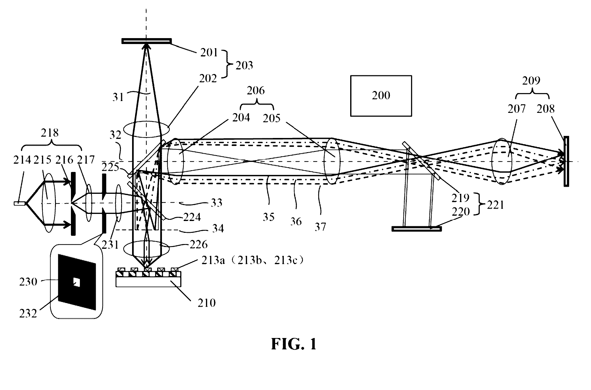
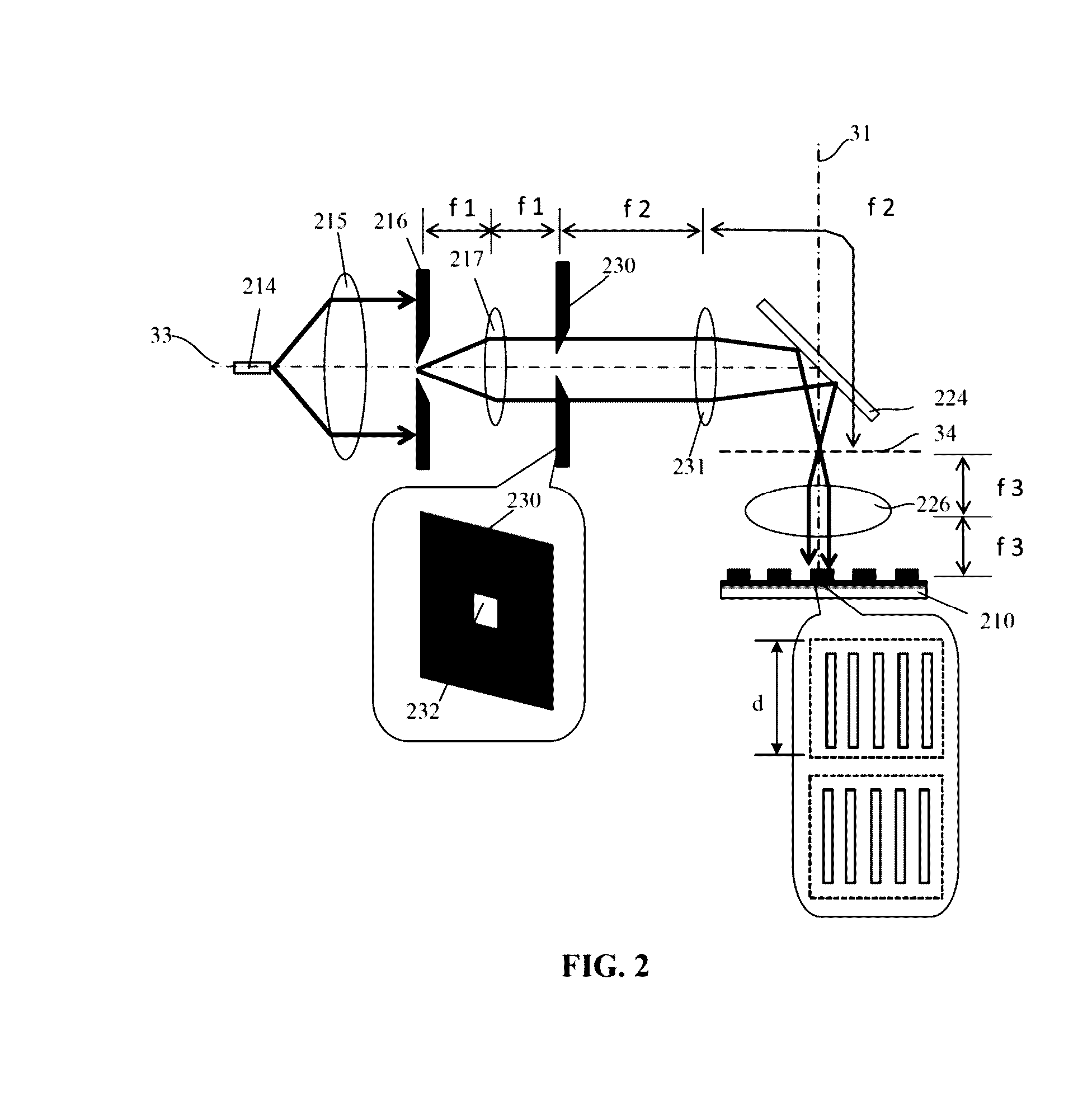
[0016]FIGS. 1-2 illustrate an exemplary overlay measurement apparatus consistent with the disclosed embodiments. As illustrated in FIG. 1, the overlay measurement apparatus includes a main control unit 200 and an illuminating unit 218.

[0017]The main control unit 200 may control the operation of the overlay measurement apparatus including, sending and receiving control signals, data processing, and display of related data, etc. The main control unit 200 may include a computer, and related circuits, etc.

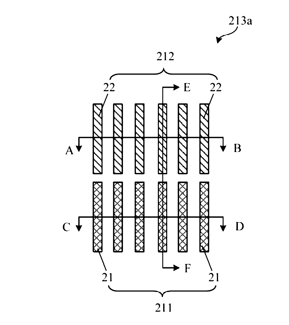
[0018]The illuminating unit 218 may generate light to illuminate the first overlay marker 213a, the second overlay marker 213b and / or the third overlay marker 213c formed on a wafer 210. For example, reflected light may be generated w...


PUM

PropertyMeasurementUnit
angleaaaaaaaaaa
angleaaaaaaaaaa
wedged angleaaaaaaaaaa

Abstract

The present disclosure provides apparatus and methods for overlay measurement. An exemplary overlay measurement apparatus includes an illuminating unit configured to generate illuminating light to illuminate a first overlay marker formed on a wafer to generate reflected light; and a first measuring unit configured to receive the reflected light from the first overlay marker to cause the reflected light to laterally shift and shear to generate interference light, to receive the interference light to form a first image, and to determine existence of an overlay offset and an exact value of the overlay offset, according to the first image.

Description

CROSS-REFERENCES TO RELATED APPLICATIONS[0001]This application claims the priority of Chinese patent application No. 201510199057.3, filed on Apr. 23, 2015, the entirety of which is incorporated herein by reference.FIELD OF THE INVENTION[0002]The present invention generally relates to the field of semiconductor manufacturing and, more particularly, relates to overlay measurement apparatus and overlay measurement methods thereof.BACKGROUND[0003]Photolithography is a major process for the fabrication of integrated circuits (ICs). A photolithography process transfers patterns on a reticle to a photoresist layer formed on a substrate.[0004]The photolithography process is usually performed by a photolithography apparatus. The photolithography apparatus includes a wafer stage for loading a substrate; a reticle stage, disposed above the wafer stage, for loading a reticle; a light source, disposed above the reticle, for providing the exposure light; and an optical projection unit, disposed ...

Claims


Application Information

Patent Timeline
Patent Type & Authority Applications(United States)
IPC IPC(8): G01B11/27G03F7/20G01B9/02
CPCG01B11/272G03F7/70633G01B9/02098G03F9/7088
Inventor LIU, YANGWU, QIANGYUE, LIWAN
Owner SEMICON MFG INT (SHANGHAI) CORP
Why Eureka
Try Eureka