Magnetic measuring device

a measuring device and magnetic field technology, applied in the direction of magneto-optic devices, magnetic field measurement, instruments, etc., can solve the problems of large optical system volume, too large device size,

Inactive Publication Date: 2016-10-27
RENESAS ELECTRONICS CORP
View PDF6 Cites 73 Cited by
  • Summary
  • Abstract
  • Description
  • Claims
  • Application Information

AI Technical Summary

Benefits of technology

[0009]A magnetic measuring device according to an embodiment detects a magnetic field intensity from a change of a fluorescent light intensity. The magnetic measuring device includes a diamond crystal, a microwave unit, a light source unit, an image sensor, a signal processing unit, and a control unit.
[0010]The diamond crystal includes a plurality of nitrogen-vacancy pairs. The microwave unit irradiates the diamond crystal with the m

Problems solved by technology

Tis manner has such a problem that the dichroic mirror also has a wide area, which results in a large volume of the optical system.
For example, in a wearable diagnostic device which c

Method used


Image

  • Magnetic measuring device
  • Magnetic measuring device
  • Magnetic measuring device

Examples


first embodiment

[0039]

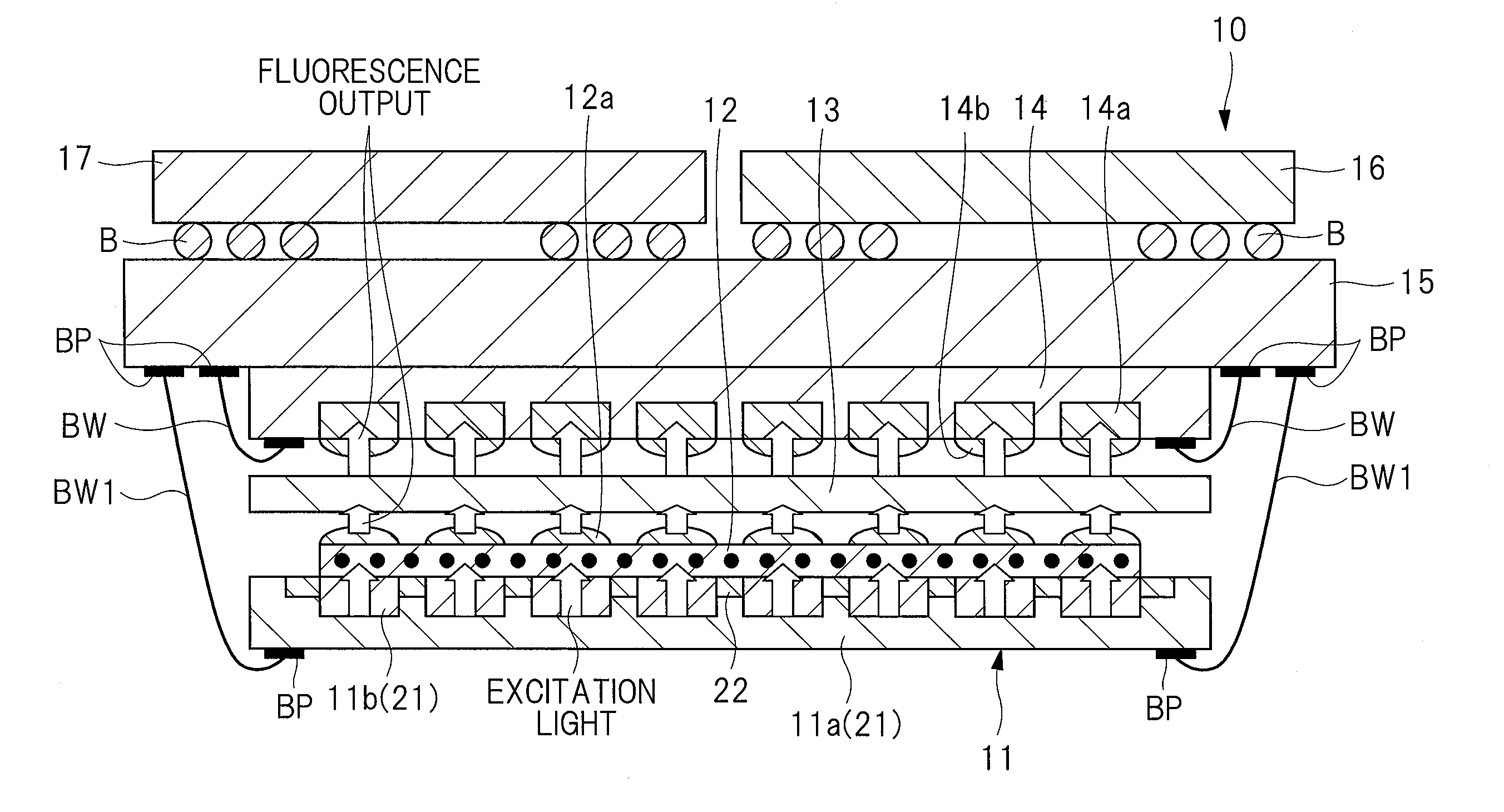
[0040]FIG. 1 is an explanatory diagram illustrating a configuration example in a magnetic measuring device 10 according to the present first embodiment.

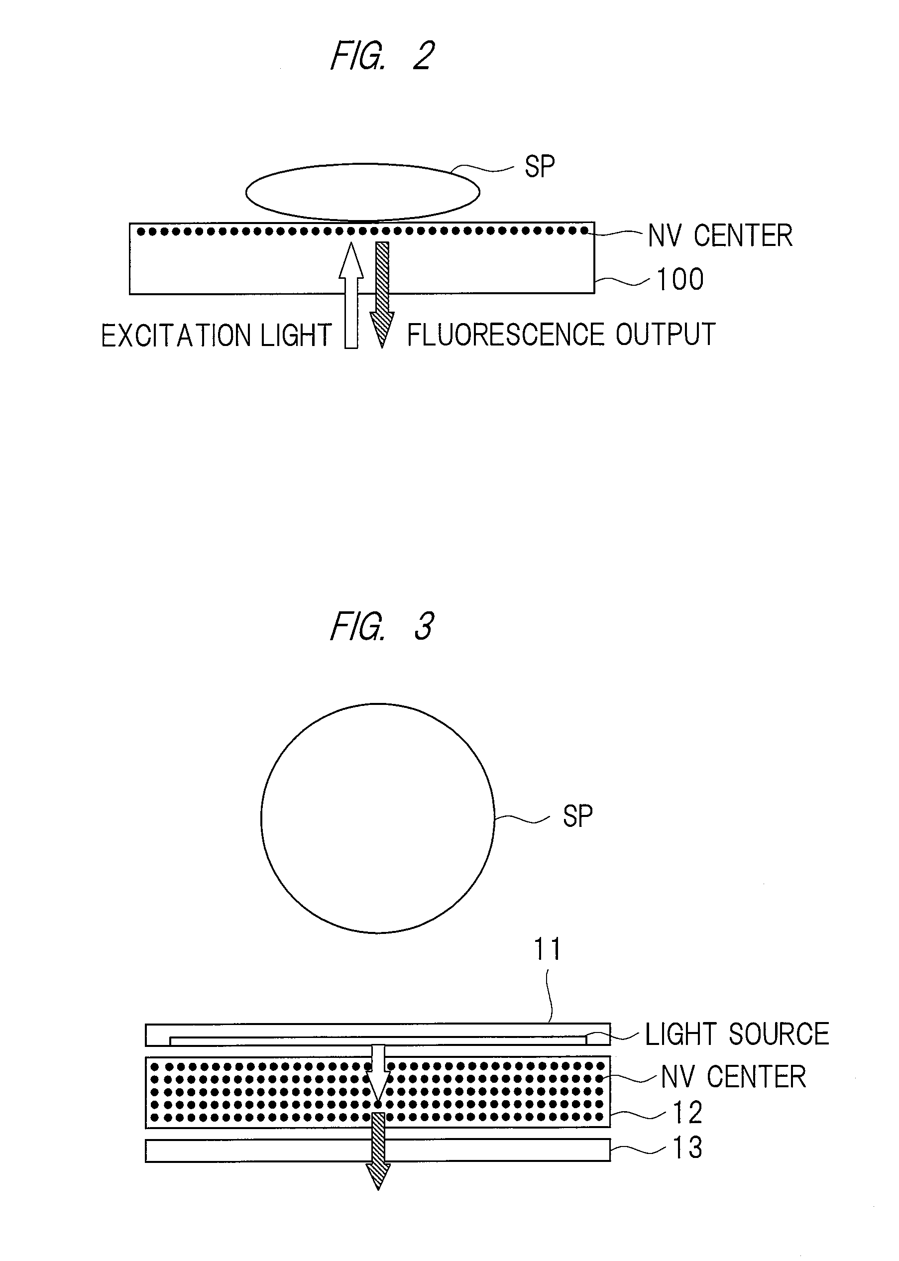
[0041]A magnetic measuring device 10 is a biomagnetic detecting device used in a medical instrument such as a magnetoencephalograph, a magnetocardiograph, and a magnetomyograph which are biomagnetic measuring devices. For example, the magnetoencephalography noninvasively measures and analyzes a weak magnetic field generated along with nervous activity of the brain over the scalp.

[0042]The magnetic measuring device 10 is made up of such a configuration as a mirrorless module so that the magnetic measuring device 10 is thinned and downsized.

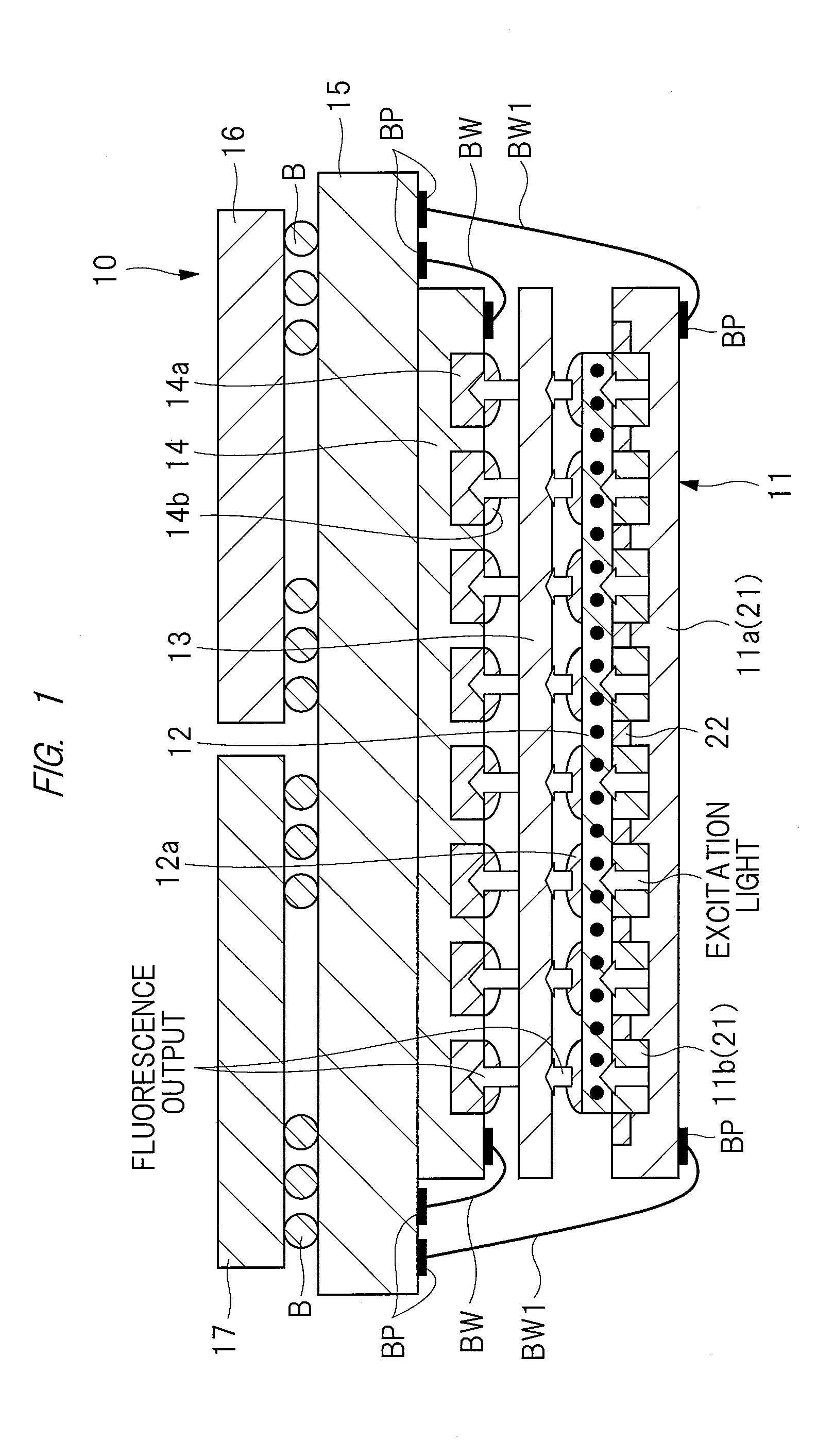
[0043]As illustrated in FIG. 1, the magnetic measuring device 10 is made up of a configuration provided with a light source array / microwave circuit chip 11, a diamond crystal 12, a filter thin film 13, an image sensor 14, a package substrate 15, a signal controller 16 and a microwave source 17...

second embodiment

[0100]

[0101]The above-described first embodiment has such a configuration that the magnetic measuring device contains the large area plate-shaped or deposited-on-a-chip diamond crystal. On the other hand, in the present second embodiment, a technique without the requirement of the large area diamond crystal will be described.

[0102]

[0103]FIG. 6 is an explanatory diagram illustrating a configuration example in the magnetic measuring device 10 according to the present second embodiment.

[0104]The magnetic measuring device 10 illustrated in FIG. 6 is different from the magnetic measuring device 10 of FIG. 1 according to the first embodiment in that the large area diamond crystal 12 is not provided as described above. Therefore, the magnetic measuring device 10 of FIG. 6 is made up of the light source array / microwave circuit chip 11, the filter thin film 13, the image sensor 14, the package substrate 15, the signal controller 16 and the microwave source 17.

[0105]In addition, the micro len...

third embodiment

[0114]

[0115]The magnetic measuring device 10 in the above-described second embodiment has such a configuration that the light source array unit 21 and the microwave circuit unit 22 of the light source array / microwave circuit chip 11 are mounted on one chip. On the other hand, in the present third embodiment, a case that the light source array unit 21 and the microwave circuit unit 22 are made up on different chip from each other will be described.

[0116]

[0117]FIG. 7 is an explanatory diagram illustrating a configuration example in the magnetic measuring device 10 according to the present third embodiment.

[0118]The magnetic measuring device 10 of FIG. 7 is different from FIG. 6 of the second embodiment in two semiconductor chips of a semiconductor chip configuring the light source array unit 21 and a semiconductor chip configuring the microwave circuit unit 22 as described above.

[0119]Therefore, the magnetic measuring device 10 of FIG. 7 is configured by the light source array unit 21...


PUM


Abstract

A magnetic measuring device can be downsized. The magnetic measuring device includes a diamond crystal, a microwave source, a light source array/microwave circuit chip, an image sensor, and a signal controller. The diamond crystal contains a plurality of nitrogen-vacancy pairs. The microwave source generates the microwave that is irradiated to the diamond crystal. The microwave circuit unit in the light source array/microwave circuit chip irradiates the diamond crystal with the microwave. The light source array in the light source array/microwave circuit chip irradiates the diamond crystal with excitation light. The image sensor detects an intensity of fluorescent light generated from the diamond crystal. The signal controller performs image processing of a fluorescent image taken-in by the image sensor, and controls operations of the light source array/microwave circuit chip and the microwave source. The light source array/microwave circuit chip is provided on a first surface side of the diamond crystal, and the image sensor is provided on a second surface side opposed to the first surface of the diamond crystal.

Description

CROSS-REFERENCE TO RELATED APPLICATION[0001]The present application claims priority from Japanese Patent Application No. 2015-86808 filed on Apr. 21, 2015, the content of which is hereby incorporated by reference into this application.TECHNICAL FIELD OF THE INVENTION[0002]The present invention relates to a magnetic measuring device. More particularly, the present invention relates to a technique effectively applied to magnetic field detection in an atmospheric air at a normal temperature using a nitrogen-vacancy pair of a diamond crystal.BACKGROUND OF THE INVENTION[0003]A diamond crystal containing a nitrogen-vacancy pair has been proposed as a high sensitivity magnetic field measuring device which can be operated in an atmospheric air at a normal temperature (see, for example, C. Müller, X. Kong, J. -M. Cai, K. Melentijević, A. Stacey, M. Markham, D. Twitchen, J. Isoya, S. Pezzagna, J. Meijer, J. F. Du, M. B. Plenio, B. Naydenov, L. P. McGuinness & F. Jelezko, “Nuclear magnetic res...

Claims


Application Information

Patent Timeline
IPC IPC(8): G01R33/032G01N21/64
CPCG01R33/032G01N21/64G01N2201/062G01N2201/06113G01N21/6456G01R33/1284
Inventor HATANO, YUJIUENO, JUNYOSHINO, TAKASHI
Owner RENESAS ELECTRONICS CORP
Why Eureka
Try Eureka