Supercharge Your Innovation With Domain-Expert AI Agents!

Chip package and manufacturing method thereof

a technology of chip package and manufacturing method, which is applied in the direction of electrolysis components, inductances, contact devices, etc., can solve the problems of difficult to reduce the cost of inductors, design inconvenience, and large assembly time of rf sensors, so as to enhance design convenience and save assembly time of chip packages. cost

Active Publication Date: 2016-10-27
XINTEC INC
View PDF0 Cites 0 Cited by
  • Summary
  • Abstract
  • Description
  • Claims
  • Application Information

AI Technical Summary

Benefits of technology

The present invention relates to a chip package which has both active and passive components. By using a redistribution layer with a passive component portion, the chip package can function as an inductor without the need for a separate inductor. This saves time and money during manufacturing and improves design flexibility. The chip package can be used as an RF sensor and does not require a separate inductor.

Problems solved by technology

However, it leads to a lot of assembly time for the RF sensor, and makes it difficult to reduce the cost of the inductors.
Moreover, additional space and circuits need to be reserved on the printed circuit board, thereby causing design inconvenience.

Method used


Image

  • Chip package and manufacturing method thereof
  • Chip package and manufacturing method thereof
  • Chip package and manufacturing method thereof

Examples


Embodiment Construction

[0042]Reference will now be made in detail to the present embodiments of the invention, examples of which are illustrated in the accompanying drawings. Wherever possible, the same reference numbers are used in the drawings and the description to refer to the same or like parts.

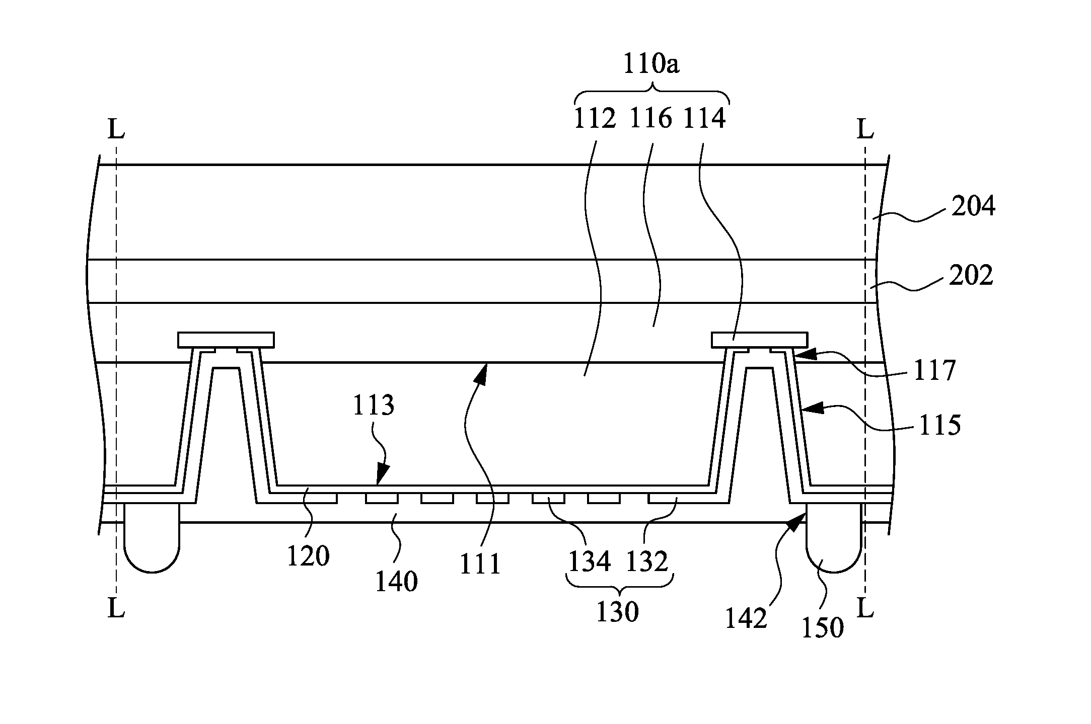
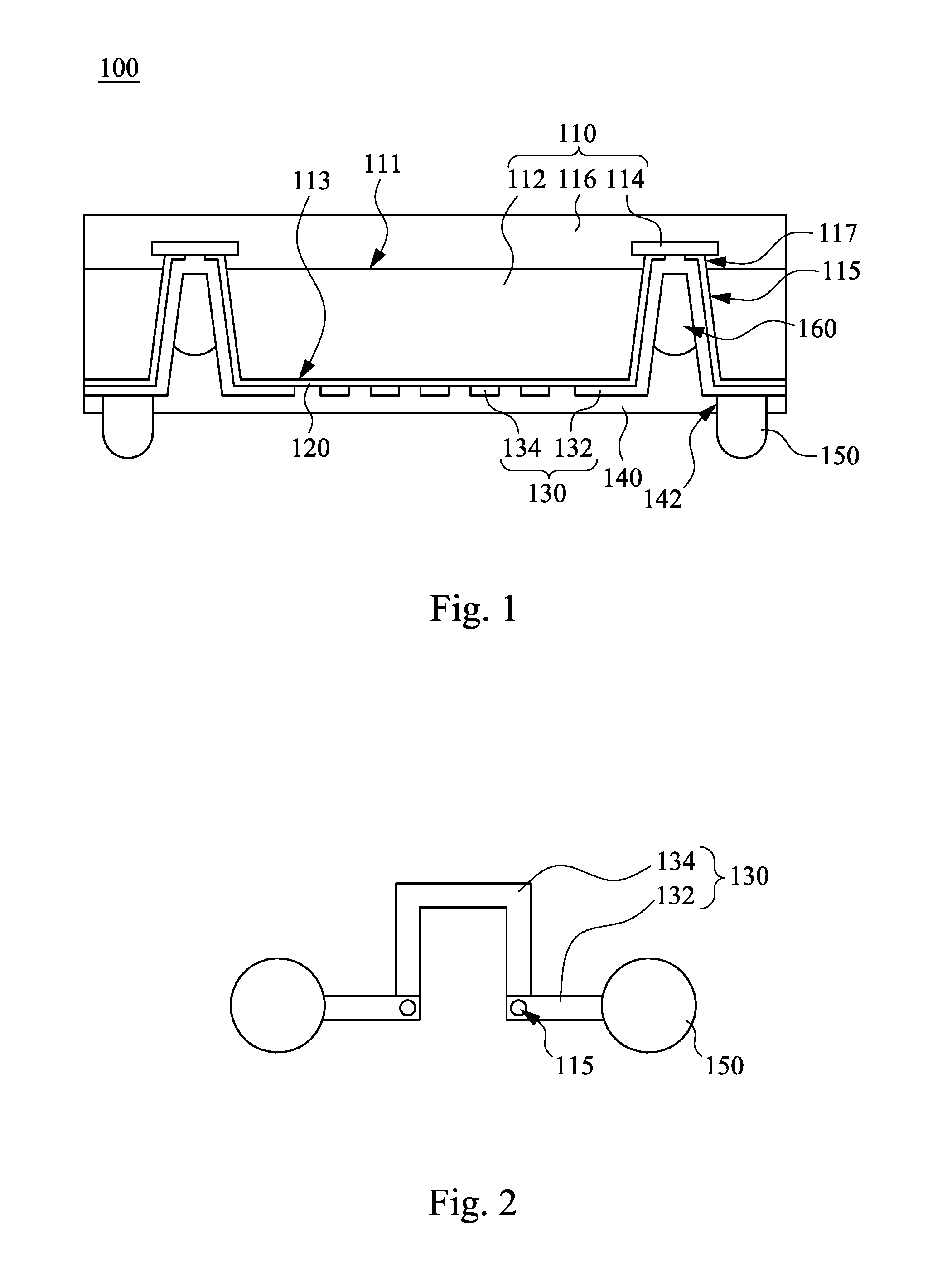
[0043]FIG. 1 is a cross-sectional view of a chip package 100 according to an embodiment of the present invention. FIG. 2 is a schematic view of a layout of a redistribution layer 130 of the chip package 100 shown in FIG. 1. As shown in FIG. 1 and FIG. 2, the chip package 100 includes a chip 110, an isolation layer 120, and a redistribution layer (RDL) 130. The chip 110 has a substrate 112, an electrical pad 114 and a protection layer 116. The substrate 112 has a first surface 111 and an opposite second surface 113. The protection layer 116 is located on the first surface 111. The electrical pad 114 is located in the protection layer 116. The substrate 112 has a through hole 115, and the protection layer 116 ha...


PUM


Abstract

A chip package includes a chip, an isolation layer, and a redistribution layer. The chip has a substrate, an electrical pad, and a protection layer. The substrate has a first surface and a second surface. The substrate has a through hole, and protection layer has a concave hole, such that the electrical pad is exposed through the concave hole and the through hole. The isolation layer is located on the second surface, the sidewall of the through hole, and the sidewall of the concave hole. The redistribution layer includes a connection portion and a passive element portion. The connection portion is located on isolation layer and in electrical contact with the electrical pad. The passive element portion is located on isolation layer that is on second surface, and an end of passive element portion is connected to connection portion that is on the second surface.

Description

RELATED APPLICATIONS[0001]This application claims priority to U.S. Provisional Application Ser. No. 62 / 153,400 filed Apr. 27, 2015, and Taiwan Application Serial Number 104126716, filed Aug. 17, 2015, the disclosures of which are incorporated herein by reference in their entireties.BACKGROUND[0002]1. Field of Invention[0003]The present invention relates to a chip package and a manufacturing method of the chip package.[0004]2. Description of Related Art[0005]A typical RF sensor includes a chip package and passive components. The passive components can be, for example, inductors. And the chip package is used as an active component. Both the chip package and the inductors are disposed on a printed circuit board, and the inductors are placed outside the chip package.[0006]That is to say, after the chip package is manufactured, additional and independent inductors are required to be arranged on the printed circuit board to allow the RF sensor working properly. However, it leads to a lot ...

Claims


Application Information

Patent Timeline
IPC IPC(8): H01L23/498H01L21/687H01L49/02H01L21/48
CPCH01L23/49838H01L23/498H01L23/49811H01L23/49827H01L28/10H01L21/4853H01L21/4846H01L21/68721H01L21/486H01L23/525H01L23/53214H01L23/53228C25D17/06H01L2224/11H01L23/5227H01L23/481H01L21/76898H01L21/2885C25D17/005C25D17/001
Inventor HO, YEN-SHIHCHANG, SHU-MINGSHEN, HSING-LUNGSU, YU-HAOWU, KUAN-JUNGCHENG, YI
Owner XINTEC INC
Features
  • R&D
  • Intellectual Property
  • Life Sciences
  • Materials
  • Tech Scout
  • Unparalleled Data Quality
  • Higher Quality Content
  • 60% Fewer Hallucinations
Learn More