Method of detecting photolithographic hotspots

a photolithographic image and hotspot detection technology, applied in image enhancement, image analysis, instruments, etc., can solve the problems of layout regions still having imaging problems, defects affecting it is difficult to fabricate the desired layout patterns on the substrate. , to achieve the effect of improving the overall image fidelity, improving precision and accuracy, and effective and quick

Active Publication Date: 2016-11-03
POWERCHIP SEMICON MFG CORP
View PDF1 Cites 2 Cited by
  • Summary
  • Abstract
  • Description
  • Claims
  • Application Information

AI Technical Summary

Benefits of technology

[0009]In the light of the need for implementation, the present invention proposes a novel method for detecting a photolithographic hotspot and is characterized in that the layout data with or without the optical proximity correction undergo an aerial image simulation to extract multiple specific aerial image intensity indices and to accordingly generate multiple aerial image detectors of various meanings in order to determine various and corresponding photolithographic hotspots. The method of the present invention may go with a conventional critical dimension (CD) check after the optical proximity correction to provide an image calibration of better precision and accuracy to greatly improve the overall image fidelity. The method involves a process flow which is relatively effective and quick and is suitable for the verification of the optical proximity correction on full chip.

Problems solved by technology

The shrinkage of the critical dimension of the circuit elements makes it harder and harder to fabricate the desirable layout patterns on the substrate.
Diffraction of light may partially account for the cause of defects during the lithographic process so that the desirable images fail to be precisely formed on the substrate, and further the defects land in the final element structures.
However, what is insufficient is that, some layout regions still have imaging problems in spite of the above resolution enhancement techniques.
Although the optical proximity correction or a process window simulation may serve as a guidance of retargeting, the entire amending flow is time-consuming and expensive.

Method used


Image

  • Method of detecting photolithographic hotspots
  • Method of detecting photolithographic hotspots
  • Method of detecting photolithographic hotspots

Examples


Embodiment Construction

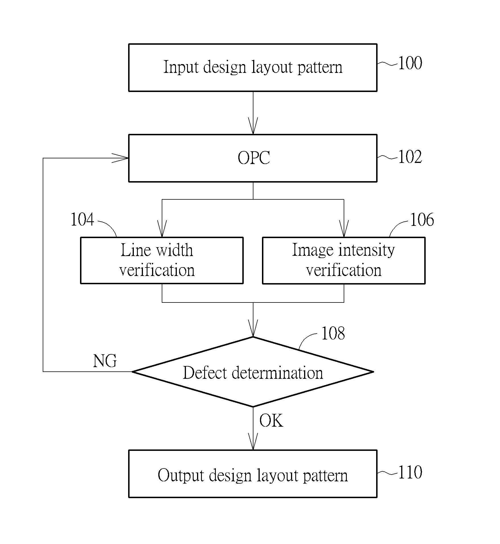
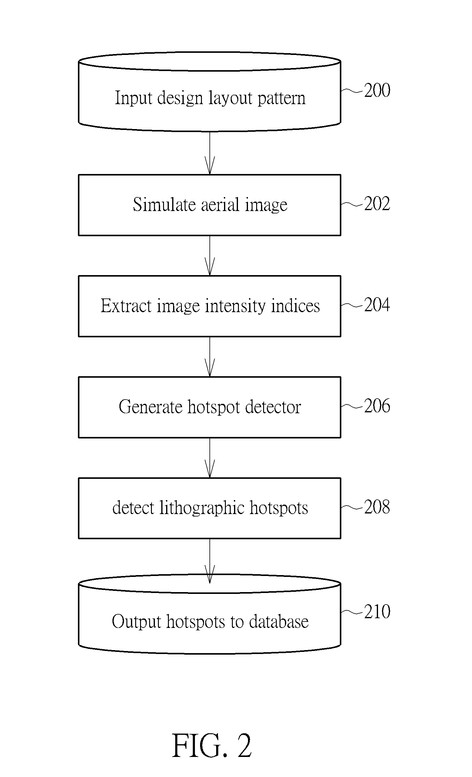
[0017]The present invention in various aspects relates to aerial images in lithography. The present invention may be variously modified and may have various embodiments. Particular embodiments of the present invention will be described in detail in the Detailed Description. However, the present invention is not limited to the particular embodiments and may be understood that the present invention includes any modification, equivalents, or alternatives that are included in the spirit and scope of the present invention. In the description of the present invention, if it is considered that a detailed description about related disclosed art makes the present invention unclear, it will not be presented herein.

[0018]Some techniques described in the specification may be implemented by means of software commands stored in a computer-readable medium, software commands operating in a computer or the combination thereof. For example, some techniques disclosed in the specification are for use i...


PUM


Abstract

A method for detecting photolithographic hotspots is disclosed. After receiving layout data, an aerial image simulation is conducted to extract aerial image intensity indices. Based on the combination of one or more aerial image intensity indices, various aerial image detectors are generated. The value of aerial image detectors is verified to determine the position and type of the photolithographic hotspots.

Description

CROSS REFERENCE TO RELATED APPLICATION[0001]This application claims priority from Taiwanese Patent Application No. 104113937, filed on Apr. 30 2015, the contents of which are hereby incorporated by reference in their entirety for all purposes.BACKGROUND OF THE INVENTION[0002]1. Field of the Invention[0003]The present invention generally relates to a method for detecting a hotspot in a photolithographic image. In particular, the present invention is directed to a method for detecting a hotspot in a photolithographic image according to aerial image intensity-related indices.[0004]2. Description of the Prior Art[0005]Electric circuits, for example integrated circuits (IC), are widely used in various electronic products, such as cars, microwave ovens, or personal computers. The design and fabrication of an IC component involves many steps, and sometimes it is called a design flow. A particular step in a design flow usually depends on the types, the complexity, the design team, the manuf...

Claims


Application Information

Patent Timeline
Patent Type & Authority Applications(United States)
IPC IPC(8): G06T7/00G06T5/00G06K9/46
CPCG06T7/0004G06T7/0042G06T2207/30148G06T7/0085G06T5/00G06K9/4604
Inventor CHANG, YI-SHIANGLIN, CHIA-CHIYEH, SHIN-SHINGSHIH, PEI-SHANLAI, JUN-CHENG
Owner POWERCHIP SEMICON MFG CORP
Why Eureka
Try Eureka