

Bidirectional insulated gate bipolar transistor
a bipolar transistor and insulated gate technology, applied in the direction of basic electric elements, electrical equipment, semiconductor devices, etc., can solve problems affecting the performance of devices, and achieve the effect of improving forward conduction characteristics
- Summary
- Abstract
- Description
- Claims
- Application Information
AI Technical Summary
Benefits of technology
Problems solved by technology
Method used
Image

Examples
Embodiment Construction
[0026]For further illustrating the invention, experiments detailing a bidirectional IGBT are described below. It should be noted that the following examples are intended to describe and not to limit the invention.
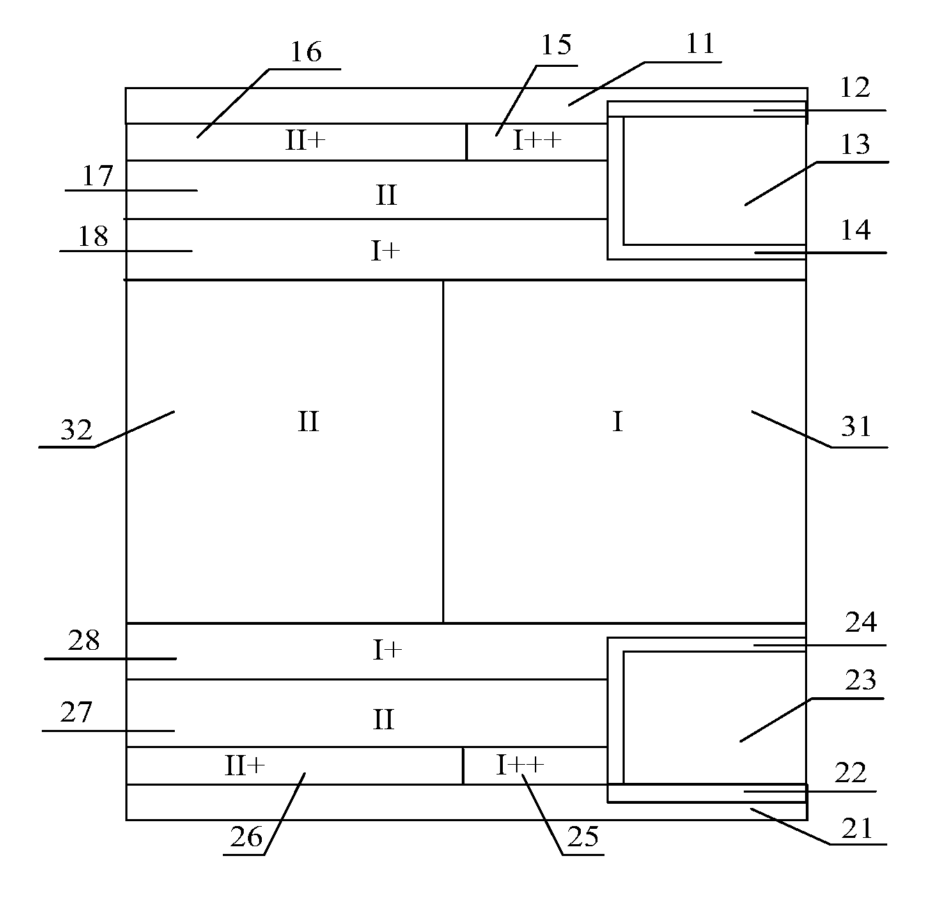
[0027]A first bidirectional IGBT is shown in FIG. 2. A cellular structure of the first bidirectional IGBT comprises two MOS structures symmetrically disposed on a top surface and a back surface of a substrate drift layer. Each MOS structure comprises: a body region 17 or 27, a heavily doped source region 15 or 25 disposed in the body region 17 or 27, and a body contact region 16 or 26 disposed in the body region 17 or 27. The heavily doped source region 15 or 25 and the body contact region 16 or 26 are independent from each other, and both surfaces of the heavily doped source region 15 or 25 and the body contact region 16 or 26 are connected to each of two metal electrodes 11 or 21. Each MOS structure further comprises a gate structure. Each gate structure is a trench-gate ...
PUM
 Abstract
Description
Claims
Application Information