Anode plate for a field emission display device

an emission display and anode plate technology, applied in the direction of cathode-ray/electron beam tube electrical connection, discharge tube luminescnet screen, tube with screen, etc., can solve the problem of defective display panels, no study of the pattern of the anode conducting band, and the use of the flexibility of the electrically conductive layer. , to achieve the effect of enhancing the sealing strength between the plates and facilitating the operation of the display circui

Inactive Publication Date: 2005-03-03
IND TECH RES INST
View PDF7 Cites 8 Cited by
  • Summary
  • Abstract
  • Description
  • Claims
  • Application Information

AI Technical Summary

Benefits of technology

[0006] The object of the present invention is to provide an anode plate for a field emission display device so that any crack occurring during the high temperature sealing process of the catho...

Problems solved by technology

However, part of the anode conducting band, e.g. the ITO layer, needs to be exposed outside the active area for connecting, so it might contact the frits and therefore be damaged during the high temperature sealing process.
As a result, the operation of circuits in the display is hindered.
This crack will further obstruct the construction of vacuum space between the anode and cathode plate...

Method used


Image

  • Anode plate for a field emission display device
  • Anode plate for a field emission display device
  • Anode plate for a field emission display device

Examples


embodiment 1

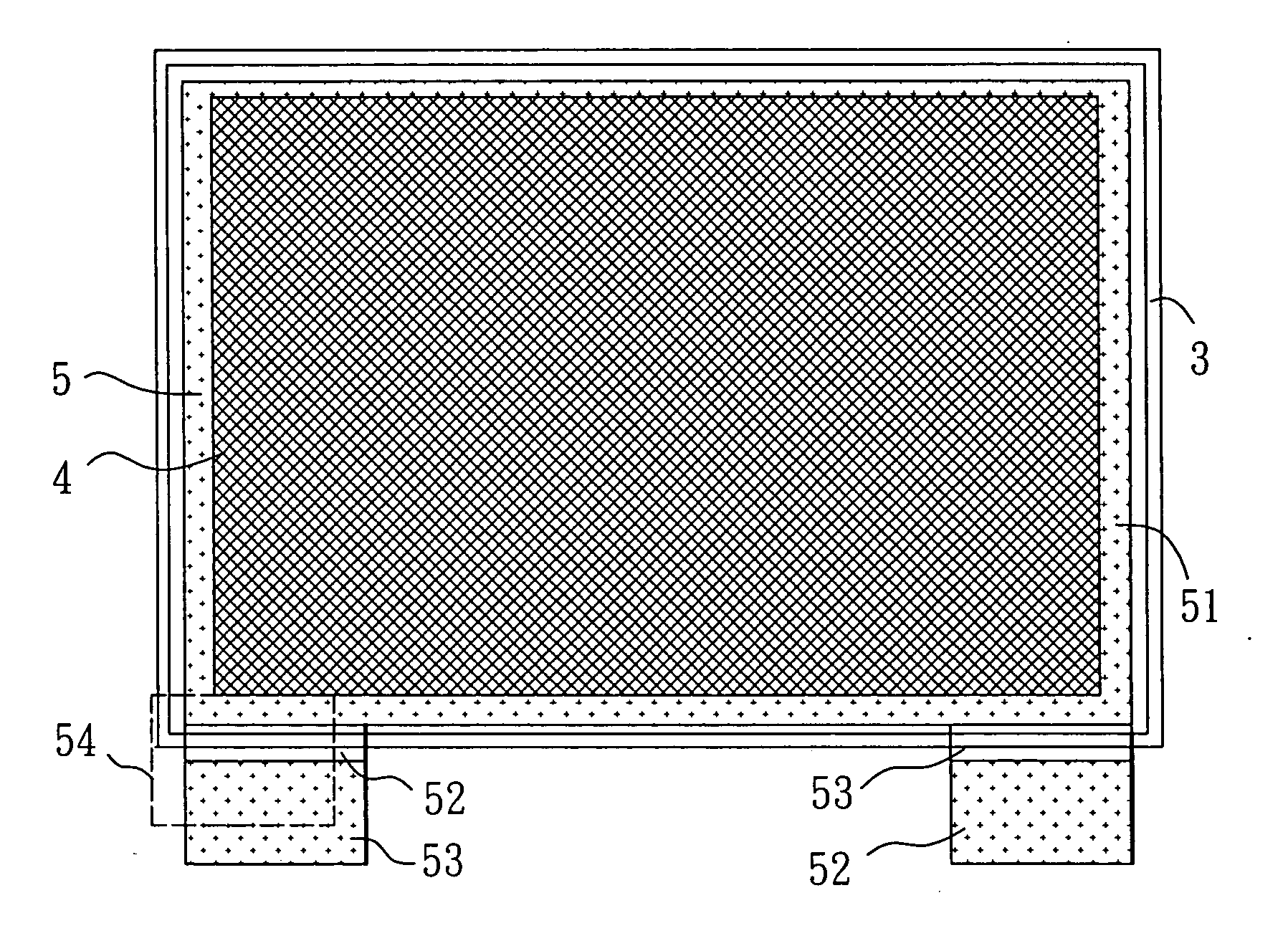
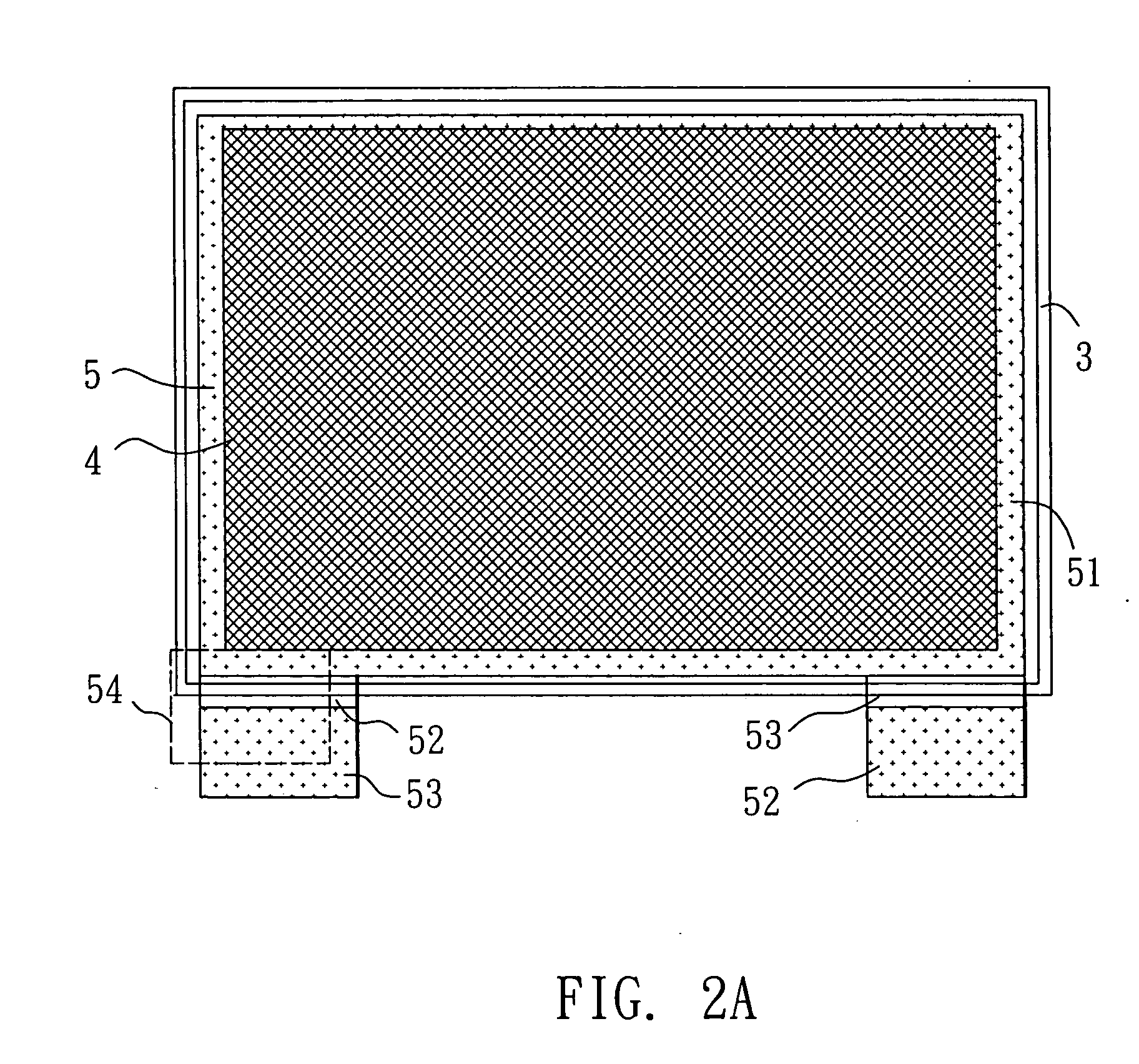
[0021] With reference to FIGS. 2A, 2B, and 2C, there are shown the sealing of the cathode plate and the anode plate having an interspacing conductive band of one preferred embodiment of the present invention. FIG. 2B is the enlarged view of block 54 in FIG. 2A. In the present embodiment, on the cathode plate 1 of the field emission display device, there are formed a plurality of carbon nanotubes for generating the electrons and a plurality of transistors (not shown). Each of the transistors is corresponding to one of the carbon nanotubes respectively and controls the switches of the pixel. A fluorescent layer 4 and an electrically conductive layer 5 are formed on the anode plate 2. The electrically conductive layer 5 is a patterned ITO glass, which is formed through thin film deposition followed by a photolithography process. The electrically conductive layer 5 includes an anode conductive layer 51 and an interspacing conductive band 52, wherein the anode conductive layer 51 is sand...

embodiment 2

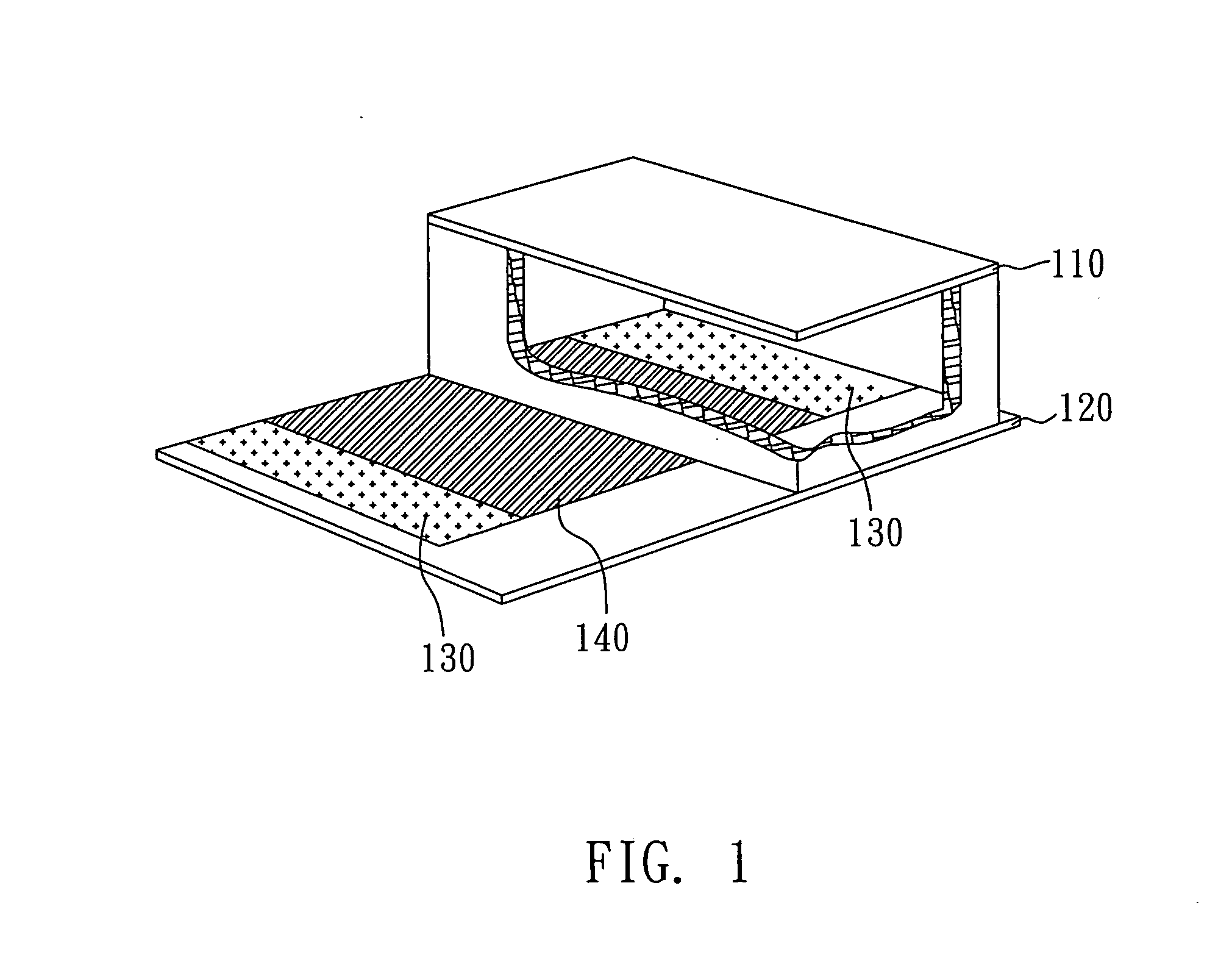
[0023] With reference to FIG. 4, there is shown the sealing of the cathode plate and the anode plate having an interspacing conductive band of another preferred embodiment of the present invention. The field emission display device of the present embodiment includes the cathode plate 21, the anode plate 22, the side frame 23 mounted between the cathode plate 21 and the anode plate 22 for forming a fixed space between the cathode plate 21 and the anode plate 22, a fluorescent layer formed at the inner side of the side frame 23 on the anode plate 22, an adhesive layer, e.g. a frit layer sandwiched between the cathode plate 21 and the side frame 23 as well as the anode plate 22 and the side frame 23 for bonding and sealing, a plurality of carbon nanotubes located on the cathode plate 21 for generating the electrons, and a plurality of transistors also located on the cathode plate 21 for controlling the switches of the pixel of the field emission display device. The electrically conduct...


PUM


Abstract

An anode plate for a field emission display device (FED) is disclosed, which has a substrate; an anode conductive layer formed on the substrate; at least one interspacing conductive band having a plurality of internal gaps for connecting the anode conductive layer and external cable lines, wherein the interspacing conductive band covers a part of the anode conductive layer; and a fluorescent layer located on the anode conductive layer, to serve as a source of luminescence for a field emission display device. The field emission display device includes the anode plate aforesaid as is also disclosed.

Description

BACKGROUND OF THE INVENTION [0001] 1. Field of the Invention [0002] The present invention relates to an anode plate for a field emission display device and, more particularly, to an anode plate for a carbon nanotube field emission display device with triode structure. [0003] 2. Description of Related Art [0004] The field emission display devices (FEDs) may eventually replace the conventional cathode ray tube (CRT) displays and will be widely applied to related electronic products in the coming future owing to the FED's advantages of large active area, short response time, and wide viewing angle. The luminescence principle of conventional FEDs with carbon nanotubes can be described as follows. The electrons are drawn from the tips of carbon nanotubes under the effect of an electrical field in a high vacuum circumstance around 10−6 torr and, subsequently, accelerated by the positive voltage of the anode plate to hit the fluorescent powders dispersed on the anode plate. Consequently, t...

Claims


Application Information

Patent Timeline
IPC IPC(8): H01J1/62H01J29/08H01J29/86H01J29/10H01J29/90H01J29/92H01J31/12H01J63/04
CPCB82Y10/00H01J31/123H01J29/925H01J29/085
Inventor CHEN, YING-HSIENLEE, CHENG-CHUNGHUANG, WEN-KUEILIN, WEI-YIHO, JIA-CHONGCHANG, YU-YANGHSIAO, MING-CHUNHSIAO, YUN-CHIAO
Owner IND TECH RES INST
Why Eureka
Try Eureka