Liquid crystal display panel

a technology of liquid crystal display and display panel, which is applied in the field of liquid crystal display panel, can solve the problem that the sealant part cannot be fully solidified, and achieve the effect of reducing the sealing strength between the color filter substrate and the array substrate, and being easy to pollu

Active Publication Date: 2019-03-21
SHENZHEN CHINA STAR OPTOELECTRONICS TECH CO LTD
View PDF7 Cites 0 Cited by
  • Summary
  • Abstract
  • Description
  • Claims
  • Application Information

AI Technical Summary

Benefits of technology

[0007]The technical problem to be solved by the present disclosure will be stated below. During a solidification procedure of a sealant in the prior art, ultraviolet would be shaded by a metal wiring that is arranged in a non-active area of an array substrate, and the sealant coated on a color filter substrate in a projection region of the metal wiring cannot be irradiated by the ultraviolet. As a result, this part of sealant cannot be solidified fully. Consequently, on the one hand, a liquid crystal layer of a liquid crystal display panel would easily be polluted by the non-fully solidified sealant, and on the other hand, a sealing strength between the color filter substrate and the array substrate would be reduced.

Problems solved by technology

As a result, this part of sealant cannot be solidified fully.

Method used


Image

  • Liquid crystal display panel
  • Liquid crystal display panel
  • Liquid crystal display panel

Examples


embodiment 1

[0049]In order to solve the aforesaid technical problem in the prior art, the embodiment of the present disclosure provides a liquid crystal display panel.

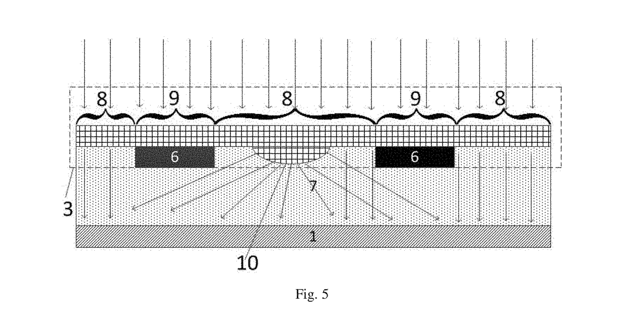
[0050]FIG. 4 schematically shows a structure of an array substrate of a liquid crystal display panel according to one embodiment of the present disclosure. FIG. 5 is a sectional view of a first non-active area of a liquid crystal display panel according to one embodiment of the present disclosure.

[0051]As shown in FIGS. 4 and 5, according to the present embodiment, the liquid crystal display panel comprises a color filter substrate 1, an array substrate 3, and a liquid crystal layer that is arranged between the color filter substrate 1 and the array substrate 3. A surface of the array substrate 3 facing the color filter substrate 1 is divided into an active area 4 and a non-active area 5. The non-active area 5 is provided with a metal wiring 6 for transmitting signal to components in the active area 4. In addition, the non-active ...

embodiment 2

[0056]FIG. 6 is a sectional view of a second non-active area of a liquid crystal display panel according to one embodiment of the present disclosure. As shown in FIG. 6, the array substrate 3 comprises a plurality of transparent layers, which comprise at least one selected transparent layer. Here, the selected transparent layer can be any transparent layer of the array substrate 3, as long as the non-flat surface 10 as stated in embodiment 1 can be formed through proper treatment. The present embodiment is not limited by this. Specifically, the selected transparent layer is preferably a flat layer, an isolating layer, or a transparent electrode layer of the array substrate 3.

[0057]At least one selected transparent layer is provided with grooves 11 in the second region 8. Here, the grooves 11 can be formed by one selected transparent layer, and can also be formed by a plurality of selected transparent layers in a superposition manner. According to the present embodiment, a quantity o...

embodiment 3

[0063]According to the present embodiment, the non-flat surface 10 as stated in embodiment 1 is formed by a transparent refraction layer arranged on the array substrate additionally. Specifically, the array substrate comprises a transparent refraction layer that is formed on a metal layer where the metal wiring is arranged. A surface of the transparent refraction layer facing the color filter substrate is non-flat in the second region. In particular, the surface of the transparent refraction layer facing the color filter substrate is provided with grooves and / or protrusions in the second region. Here, the transparent refraction layer can be formed by one insulation layer, and can also be formed by a plurality of insulation layers in a superposition manner

[0064]Specifically, FIG. 9 is a sectional view of a fifth non-active area of a liquid crystal display panel according to one embodiment of the present disclosure. As shown in FIG. 9, the array substrate 3 comprises an insulation lay...


PUM

PropertyMeasurementUnit
transparentaaaaaaaaaa
non-active areaaaaaaaaaaa
sealing strengthaaaaaaaaaa

Abstract

A liquid crystal display panel is disclosed. The liquid crystal display panel includes a color filter substrate, an array substrate, and a liquid crystal layer. A surface of the array substrate facing the color filter substrate is divided into an active area and a non-active area. The non-active area includes a second region where no metal wiring is arranged. The surface of the array substrate facing the color filter substrate is non-flat in the second region. According to the present disclosure, a sealing strength between the color filter substrate and the array substrate can be improved, and pollution on a liquid crystal layer of the liquid crystal display panel can be avoided.

Description

CROSS REFERENCE TO RELATED APPLICATION[0001]The present application claims priority of Chinese patent application CN201710081895.X, entitled “Liquid Crystal Display Panel” and filed on Feb. 15, 2017, the entirety of which is incorporated herein by reference.FIELD OF THE INVENTION[0002]The present disclosure relates to the technical field of liquid crystal display, and particularly to a liquid crystal display panel.BACKGROUND OF THE INVENTION[0003]At present, liquid crystal display technology has been widely used in various kinds of electronic products. The narrow frame technology has become a conventional technical means in the liquid crystal display field. Since the frame is narrow, an image displayed by a liquid crystal display panel is more complete, and a utilization ratio of a display screen can be improved. When an electronic product with a narrow frame liquid crystal display panel is used, such as TV, mobile phone, and tablet personal computer, a larger visual field can be ob...

Claims


Application Information

Patent Timeline
Patent Type & Authority Applications(United States)
IPC IPC(8): G02F1/1335G02F1/1362G02F1/1339
CPCG02F1/133514G02F1/133512G02F1/1339G02F1/136286G02F1/1345G02F1/13458G02F2001/13396G02F1/13394G02F1/13452G02F2001/13456G02F1/13392G02F1/133516G02F1/1362G02F1/133504G02F1/133526G02F1/1341G02F2202/023G02F1/133388G02F1/13396G02F1/13456
Inventor MENG, XIAOLONG
Owner SHENZHEN CHINA STAR OPTOELECTRONICS TECH CO LTD
Why Eureka
Try Eureka