RF power amplifiers with diode linearizer

a technology of power amplifiers and linearizers, applied in the direction of rf amplifiers, amplifier modifications to reduce non-linear distortion, negative-feedback circuit arrangements, etc., can solve the problems of non-linear performance of high-efficiency rf power amplifiers such as inverse class f, class e, and doherty amplifiers, and achieve the effect of reducing inter-modulation products

Active Publication Date: 2016-11-10
SKYWORKS SOLUTIONS INC
View PDF3 Cites 9 Cited by
  • Summary
  • Abstract
  • Description
  • Claims
  • Application Information

AI Technical Summary

Benefits of technology

[0012]According to various embodiments, an RF power amplifier circuit with an input and an output is disclosed. There may be a power amplifier transistor with a first terminal connected to the input, a second terminal connected to the output, and a third terminal. The RF power amplifier circuit may also include a linearizer circuit connected to the third terminal and to ground. The linearizer circuit may have a non-linear current-voltage curve as well as a non-linear capacitance. The linearizer circuit reduces inter-modulation products in a current through the power amplifier transistor from the second terminal to the third terminal that corresponds to an input signal applied to the input.

Problems solved by technology

High efficiency RF power amplifiers such as class F, inverse class F, class E, and Doherty amplifiers, however, all exhibit non-linear performance because of lower gate bias voltages when implemented with complementary metal oxide semiconductor (CMOS) technology.

Method used


Image

  • RF power amplifiers with diode linearizer
  • RF power amplifiers with diode linearizer
  • RF power amplifiers with diode linearizer

Examples


first embodiment

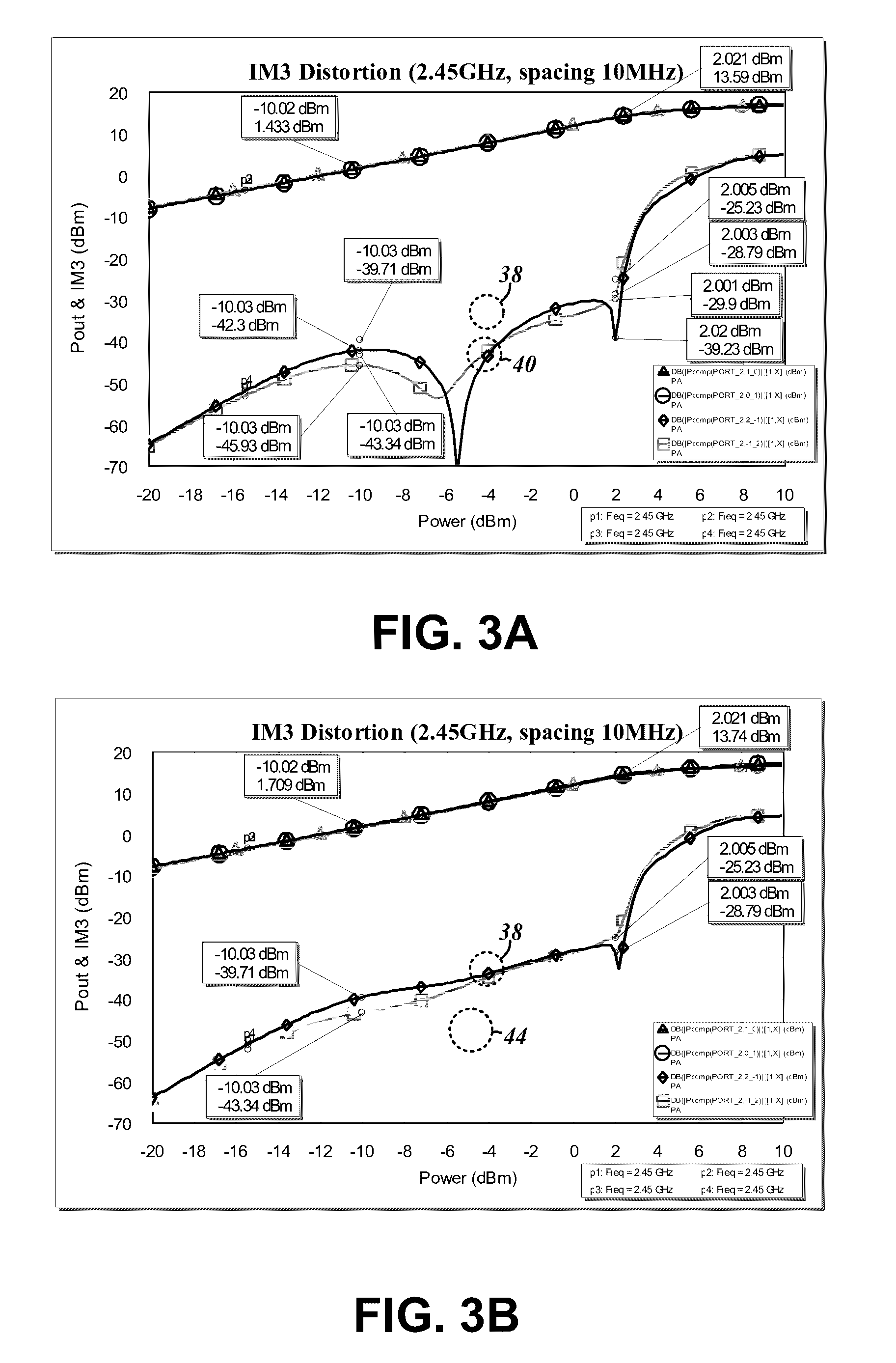
[0045]The graph of FIG. 3B likewise plots the simulated IM3 distortion at the 2.4 GHz ISM frequency for the RF power amplifier circuit 10a. However, different size diodes were simulated, in particular, relative areas of 0.15, 0.2, and 0.25. The first graph plot 38 shows the IM3 products without the diode linearizer circuit 12a, and a second plot 44 shows the reduced IM3 products with the aforementioned differently sized diodes.

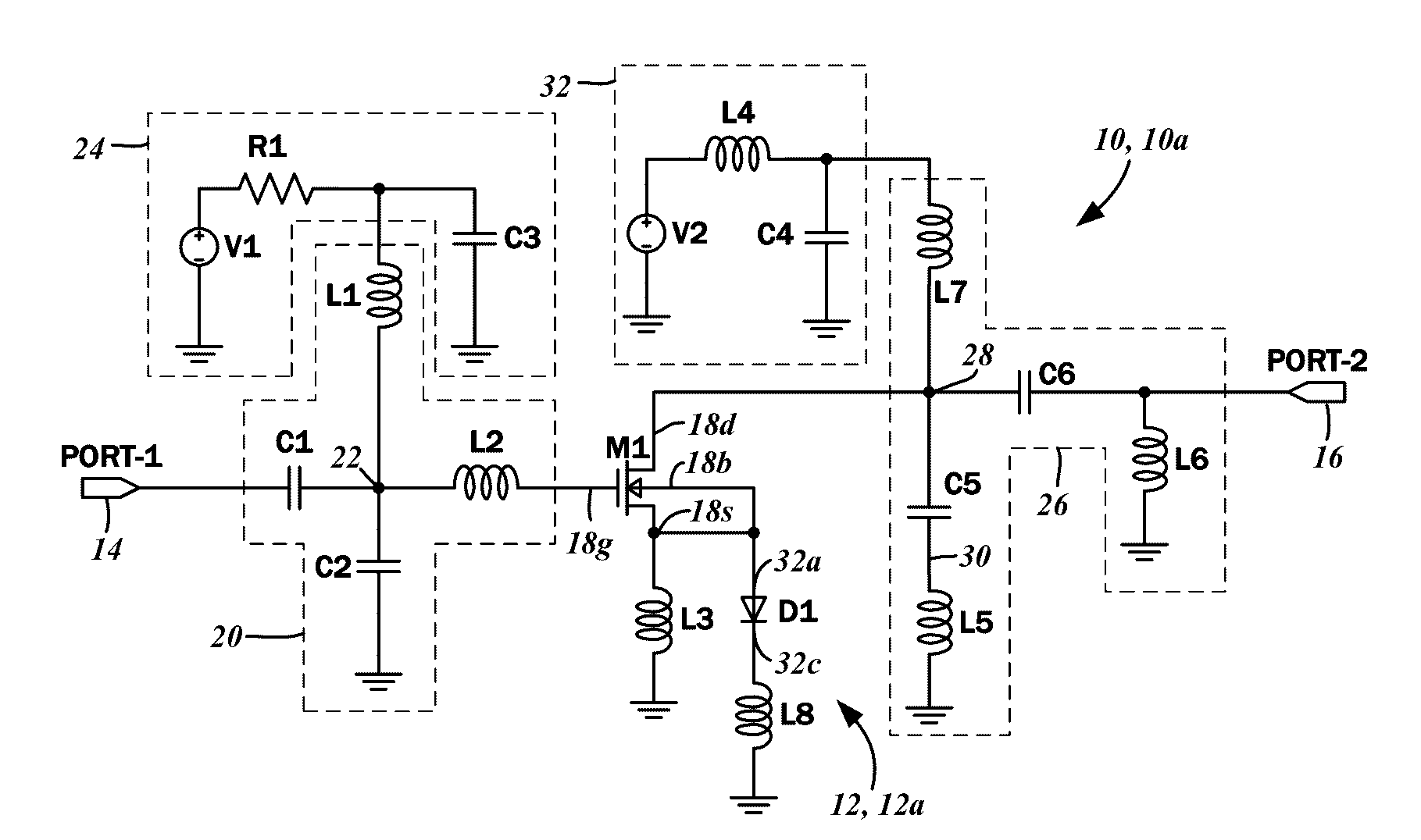
[0046]FIG. 4 is a schematic diagram of a second embodiment of the RF power amplifier circuit 10b including a second embodiment of the diode linearizer circuit 12b. Because the basic components of the RF power amplifier circuit 10b, that is, the single stage amplifier transistor M1, along with the input matching circuit, output matching circuit, the control voltage circuit, and the bias circuit are the same as in the first embodiment of the RF power amplifier circuit 10a, the details thereof will not be repeated for the sake of brevity.

second embodiment

[0047]The source terminal 18s of the transistor M1 is similarly connected to the inductor L3, along with the first diode D1 that is connected in series with the inductor L8 to ground. Additionally, however, the diode linearizer circuit 12b includes a second diode D2 that is connected in anti-parallel to the first diode D1. The anode 32a of the first diode D1 is connected to the source terminal 18s (and also connected to the body terminal 18b), while the cathode 32c of the first diode D1 is connected to the inductor L8. An anode 46a of the second diode D2 is connected to the cathode 32c of the first diode D1 and the inductor L8. A cathode 46c of the second diode D2 is connected to the anode 32a of the first diode, and the source terminal 18s of the transistor M1. Again, no direct current bias voltage is connected to the first diode D1 or the second diode D2.

[0048]The RF current through the source terminal 18s of the transistor M1 passes through a parallel circuit of the inductor L3 i...

fourth embodiment

[0059]The source terminal 18s of the transistor M1 is connected to the inductor L3, along with the first diode D1 that is connected in series with the inductor L8 to ground. In comparison to the previously described embodiments that included the second diode D2, in the diode linearizer circuit 12d, an alternative configuration is contemplated. Specifically, the second diode D2, that is, the cathode 46c thereof, is connected to the gate terminal 18g of the transistor M1. Thus, the direct current bias voltage V1 is applied to the cathode 46c of the second diode D2. As noted above, the input matching circuit 20, which is comprised of the capacitor C1, the capacitor C2, the inductor L1, and the inductor L2, is tuned to impedance match the gate terminal 18g of the transistor M1 to the RF signal source that is connected to the input port 14. With the introduction of the second diode D2 as a direct connection to the input port 14, according to certain embodiments of the present disclosure,...


PUM


Abstract

A radio frequency (RF) power amplifier circuit with a diode linearizer circuit. The power amplifier circuit has an input and an output, as well as a power amplifier transistor with a first terminal connected to the input, a second terminal connected to the output, and a third terminal. The linearizer circuit is connected to the third terminal and to ground, and has a non-linear current-voltage curve as well as a non-linear capacitance. The linearizer circuit reduces inter-modulation products in a current through the power amplifier transistor from the second terminal to the third terminal that corresponds to an input signal applied to the input.

Description

CROSS-REFERENCE TO RELATED APPLICATIONS[0001]This application relates to and claims the benefit under 35 U.S.C. §119(e) to U.S. Provisional Patent Application No. 62 / 157,896 filed May 6, 2015 and entitled “RF POWER AMPLIFIERS WITH DIODE LINEARIZER,” the entire contents of which is wholly incorporated herein by reference.STATEMENT RE: FEDERALLY SPONSORED RESEARCH / DEVELOPMENT[0002]Not ApplicableBACKGROUND[0003]1. Technical Field[0004]The present disclosure relates generally to radio frequency (RF) integrated circuits, and more particularly, to RF power amplifiers with diode linearizers.[0005]2. Related Art[0006]Generally, wireless communications involve an RF carrier signal that is variously modulated to represent data, and the modulation, transmission, receipt, and demodulation of the signal conform to a set of standards for coordination of the same. Many different mobile communication technologies or air interfaces exist, including GSM (Global System for Mobile Communications), EDGE...

Claims


Application Information

Patent Timeline
Patent Type & Authority Applications(United States)
IPC IPC(8): H03F1/32H03F1/34H03F1/56H03F3/193H03F3/21
CPCH03F1/3205H03F3/193H03F3/21H03F1/56H03F2200/15H03F2200/126H03F2200/225H03F2200/391H03F2200/451H03F1/342H03F1/565H03F3/245
Inventor GORBACHOV, OLEKSANDRZHANG, LISETTE L.MUSIOL, LOTHAR
Owner SKYWORKS SOLUTIONS INC
Why Eureka
Try Eureka