Semiconductor device
- Summary
- Abstract
- Description
- Claims
- Application Information
AI Technical Summary
Benefits of technology
Problems solved by technology
Method used
Image

Examples
first exemplary embodiment
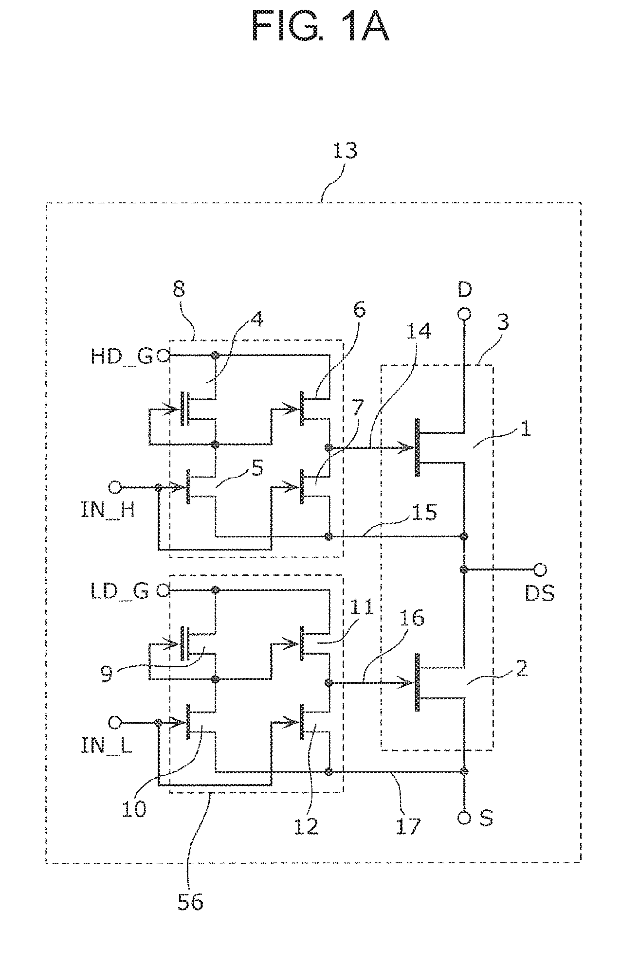
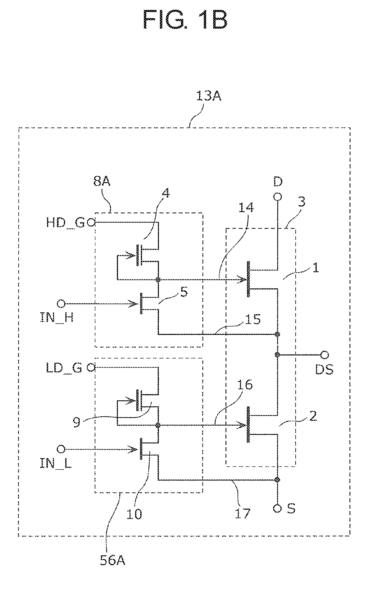
[0053]FIG. 1A is a circuit diagram of a DC-DC converter, which is a semiconductor device 13 according to the present exemplary embodiment. This circuit configuration shows a case, as one example, where a field-effect transistor formed with a nitride semiconductor is used.
[0054]Semiconductor device 13 according to the present exemplary embodiment includes power device stage 3 having a half-bridge configuration, high side gate driver 8 (a first gate driver) and low side gate driver 56 (a second gate driver).
[0055]Power device stage 3 includes high side power FET (field-effect transistor) 1 (first power transistor) and low side power FET 2 (second power transistor). A drain terminal D of high side power FET 1 is connected to a power supply (not shown) and a source terminal S of low side power FET 2 is connected to a ground (not shown) (grounded).
[0056]High side gate driver 8 includes depression type FET 4 (depression type transistor), and enhancement type FETs 5, 6 and 7 (first to thir...
modification example of first exemplary embodiment
[0098]In the following, a semiconductor device according to a modification example of the first exemplary embodiment will be described with reference to the accompanying drawings.
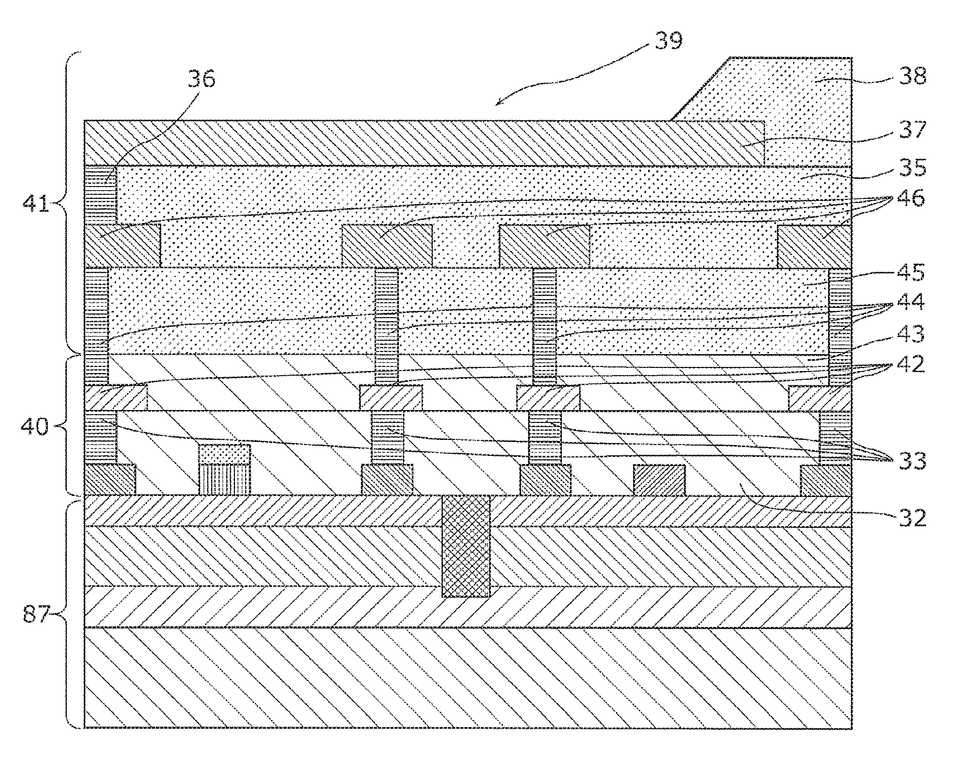
[0099]In FIG. 7, the same components as those in the structures shown in FIG. 1A to FIG. 6B are given the same reference numerals to omit description thereof. A structure shown in FIG. 7 is the same as the structure as far as primary thick film wiring 34 (or 46) shown in FIG. 6A. In FIG. 7, the arrangement of via holes 65 and 66 in high side power FET 1 and the arrangement of via holes 70 and 71 in low side power FET 2 in FIG. 6A are exchanged respectively. Also, the position of the drain electrode pad D and the source electrode pad S and the position of the drain / source electrode pad are exchanged. In other words, in this arrangement, an electrode pad with the shortest distance to the gate driver is the drain / source electrode pad DS.
[0100]While in the arrangement shown in FIG. 7, wirings with the shortest ...
second exemplary embodiment
[0102]In the following, a semiconductor device according to a second exemplary embodiment will be described with reference to the accompanying drawings. In FIG. 8, the same components as those in the structures shown in FIG. 1A to FIG. 7 are given the same reference numerals to omit description thereof. A structure shown in FIG. 8 is the same as the structure as far as primary thick film wiring 34 (or 46) shown in FIG. 6A. The structure in FIG. 8, which has approximately the same electrode pad arrangement as in FIG. 6A, is different in having drain electrode pad 72 (first electrode pad) of high side power FET 1, which pad is disposed at the shortest distance from high side gate driver 8.
[0103]Drain electrode pad 72 is an electrode pad disposed at a position closest to high side gate driver 8 among the plurality of drain electrode pads D and the plurality of drain / source electrode pads DS that high side power FET 1 has.
[0104]Drain electrode pad 72 is formed to be as small as possible...
PUM
 Abstract
Description
Claims
Application Information
 - R&D Engineer
- R&D Manager
- IP Professional
- Industry Leading Data Capabilities
- Powerful AI technology
- Patent DNA Extraction
Browse by: Latest US Patents, China's latest patents, Technical Efficacy Thesaurus, Application Domain, Technology Topic.
© 2024 PatSnap. All rights reserved.Legal|Privacy policy|Modern Slavery Act Transparency Statement|Sitemap