Ltps TFT pixel unit and manufacture method thereof

a technology of pixel units and manufacturing methods, applied in the field of display technology, to achieve the effect of preventing side effects

Active Publication Date: 2016-11-24
TCL CHINA STAR OPTOELECTRONICS TECH CO LTD
View PDF3 Cites 0 Cited by
  • Summary
  • Abstract
  • Description
  • Claims
  • Application Information

AI Technical Summary

Benefits of technology

[0004]An objective of the present invention is to provide a LTPS TFT pixel unit, which can reduce the side effect and promote the electrical property thereof.
[0019]The benefits of the present invention are: different from the condition of prior arts, the present invention forms a semiconductor pattern layer and a first insulative layer, which are located in the same layer and heights are the same so that the second insulative layer latter formed can be in a flat state without convex structures. Thus, the gate layer can be on the flat second insulative layer to ensure the consistent gap of the semiconductor pattern layer and prevent the side effects due to the uneven gap between the gate layer and the semiconductor pattern layer caused by some convex structures of the second insulative layer. Meanwhile, the electrical property of the LTPS TFT pixel unit can be promoted.

Problems solved by technology

On the other hand, the stepped structures of the buffer layer exists, the signals becomes unstable in the transmission, and thus influences the electrical property of the LTPS TFT pixel unit.

Method used


Image

  • Ltps TFT pixel unit and manufacture method thereof
  • Ltps TFT pixel unit and manufacture method thereof
  • Ltps TFT pixel unit and manufacture method thereof

Examples


Embodiment Construction

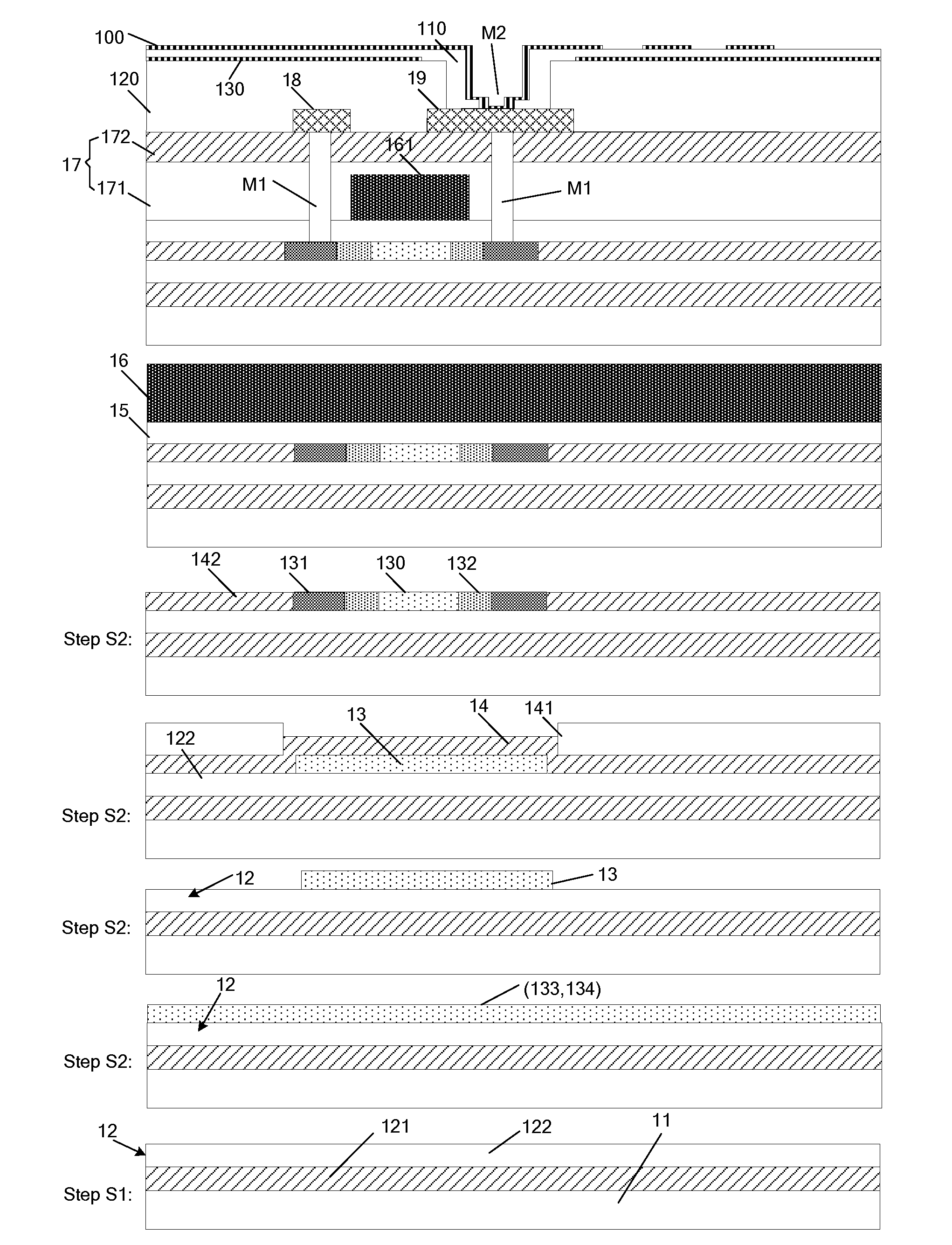
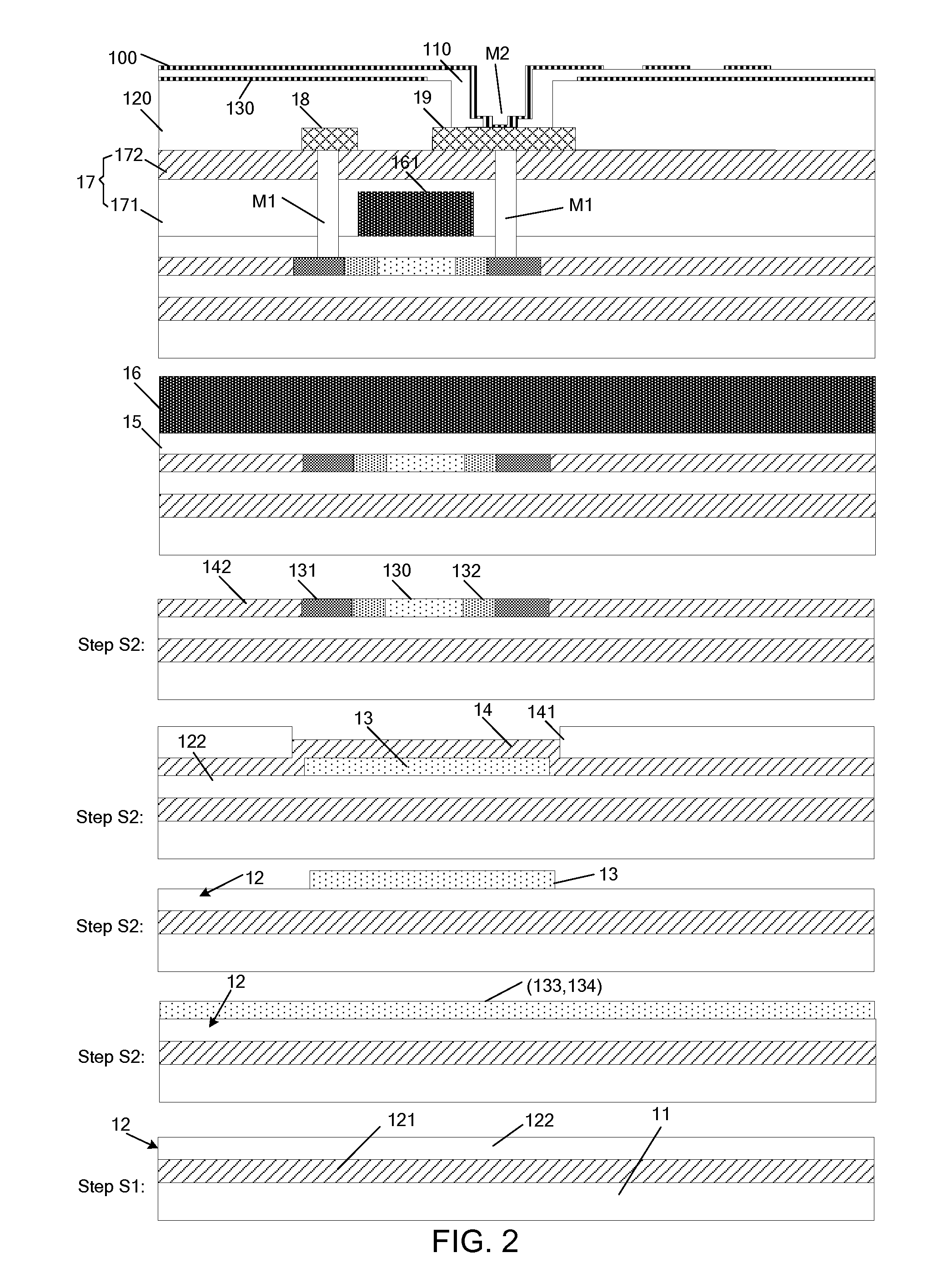
[0023]Please refer to FIG. 1 and FIG. 2. FIG. 1 is a flowchart of a manufacture method of a TFT pixel unit provided by the embodiment of the present invention, and FIG. 2 is a process diagram corresponding to the method shown in FIG. 1. As shown in FIG. 1 and FIG.2, the manufacture method provided by the embodiment of the present invention comprises steps of:

[0024]step S1, providing a substrate 11 and forming a buffer layer 12 on the substrate 11.

[0025]Specifically, a silicon nitride layer 121 and a silicon oxide layer 122 are sequentially formed on the substrate to be the buffer layer 12.

[0026]step S2, forming a semiconductor pattern layer 13 and a first insulative layer 14, and the semiconductor pattern layer 13 and the first insulative layer 142 are located in the same layer and heights of the semiconductor pattern layer 13 and the first insulative layer 142 are the same.

[0027]The step specifically is: first, an amorphous silicon layer 133 is formed on the buffer layer 12, and sp...


PUM


Abstract

The present invention discloses a LTPS TFT pixel unit and a manufacture method thereof. The method comprises steps of: providing a substrate and forming a buffer layer on the substrate; forming a semiconductor pattern layer and a first insulative layer on the buffer layer, and the semiconductor pattern layer and the first insulative layer are located in the same layer and heights of the semiconductor pattern layer and the first insulative layer are the same. With the aforesaid arrangement, the present invention can reduce the side effect of the LTPS TFT pixel unit and promote the electrical property thereof.

Description

FIELD OF THE INVENTION[0001]The present invention relates to a display technology field, and more particularly to a LTPS TFT pixel unit and a manufacture method thereof.BACKGROUND OF THE INVENTION[0002]The formation procedure of the LTPS TFT (Low Temperature Poly-silicon Thin Film Transistor) according to prior arts is: first deposing the buffer layer, and forming the semiconductor pattern layer. Furthermore, other elements of the LTPS TFT pixel unit, such as the insulative layer, the gate, etc. are formed on the semiconductor pattern layer.[0003]Because the semiconductor pattern layer is formed on the buffer layer in the LTPS TFT pixel unit according to prior arts, that is to say, the semiconductor pattern layer is convex upward from the buffer layer, and the latter formed insulative layer forms stepped convex structures at two ends of the semiconductor pattern layer. Thus, the gaps of the gate and the semiconductor pattern layer formed on the buffer layer is not even to cause side...

Claims


Application Information

Patent Timeline
Patent Type & Authority Applications(United States)
IPC IPC(8): H01L27/12H01L29/66H01L21/3105H01L21/02
CPCH01L27/1296H01L27/1262H01L27/1248H01L21/02164H01L21/0217H01L29/78621H01L21/02532H01L21/02592H01L21/02667H01L21/31055H01L29/66757H01L21/77H01L27/1214H01L29/06H01L29/6675H01L29/78627H01L27/1218H01L27/1288G02F1/13625H01L27/1222H01L27/127H01L29/78678G02F1/1333H01L27/12
Inventor YANG, ZUYOU
Owner TCL CHINA STAR OPTOELECTRONICS TECH CO LTD
Why Eureka
Try Eureka