Resolver signal detection circuit
a signal detection and circuit technology, applied in the direction of safeguarding equipment, instruments, measurement devices, etc., can solve problems such as inability to detect disconnection
- Summary
- Abstract
- Description
- Claims
- Application Information
AI Technical Summary
Benefits of technology
Problems solved by technology
Method used
Image

Examples
first embodiment
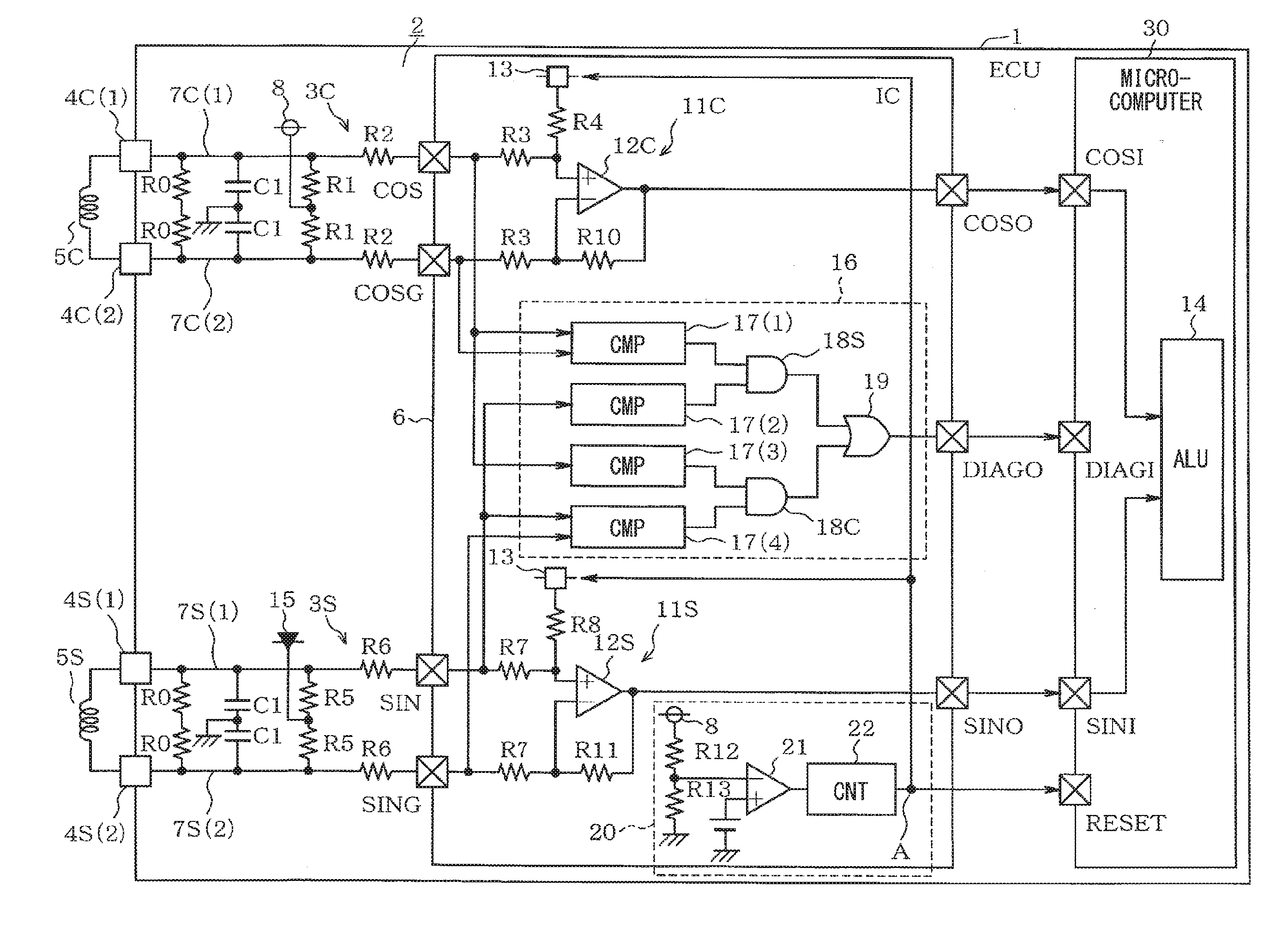
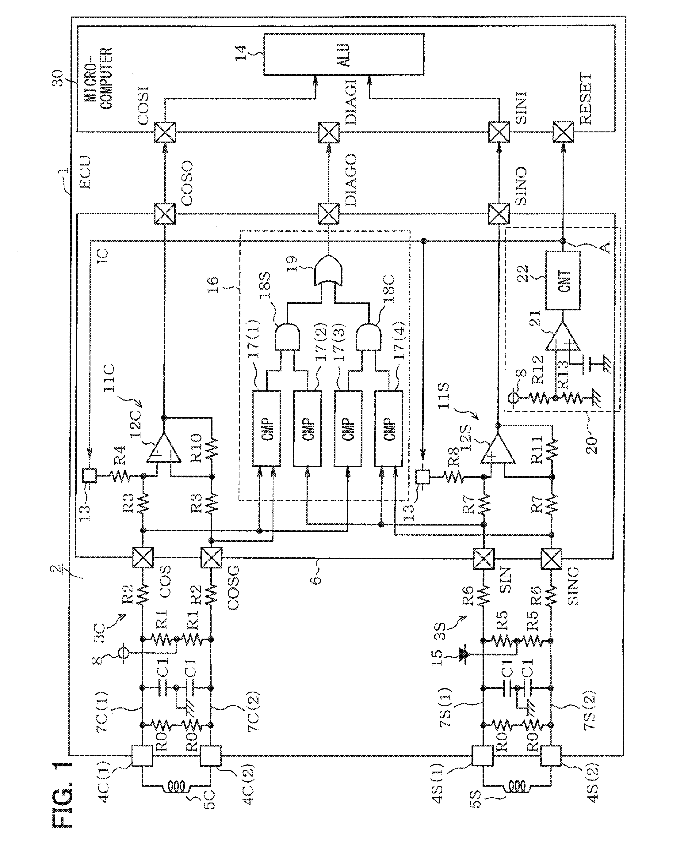
[0017]Referring first to FIG. 1, an electronic control unit (ECU) 1 includes a resolver signal detection circuit 2 and a microcomputer 30. The resolver signal detection circuit 2 includes a cosine-phase (COS-phase) detection part 3C and a sine-phase (SIN-phase) detection part 35. Input terminals 4C(1) and 4C(2) of the COS-phase detection part 3C are connected to both ends of a COS-phase coil 5C of a resolver. Input terminals 4S(1) and 4S(2) of the SIN-phase detection part 3C are connected to both ends of a SIN-phase coil 5S of the resolver.
[0018]The input terminals 4C(1) and 4C(2) and input terminals COS and COSG of an integrated circuit (IC) 6, to which a part of circuit elements of the resolver signal detection circuit 2 are connected, are connected via signal wires 7C(1) and 7C(2) as well as resistor elements R2 and R2, respectively. Between the signal wires 7C(1) and 7C(2), a series circuit of two resistor elements R0, a series circuit of two capacitors C1 and a series circuit o...
second embodiment
[0049]A second embodiment will be described below with respect to only differences from the first embodiment while designating the same structural parts as the first embodiment with the same reference numerals for simplicity of description.
[0050]In the second embodiment, as shown in FIG. 3, an ECU IN is adapted to a case, in which the DIAG signal is outputted as a low-active signal. In an IC 6N, a comparison logic part 16N is provided in place of the comparison logic part 16. The comparison logic part 16N is provided with NOR gates 23C, 235 and a NAND gate 24 in place of the AND gates 18C, 18S and the OR gate 19. Thus the DIAG signal is outputted to the microcomputer 30 as the low-active signal, The NOR gate is an AND gate operable with negative logic inputs and the NAND gate is an OR gate operable with negative logic inputs.
third embodiment
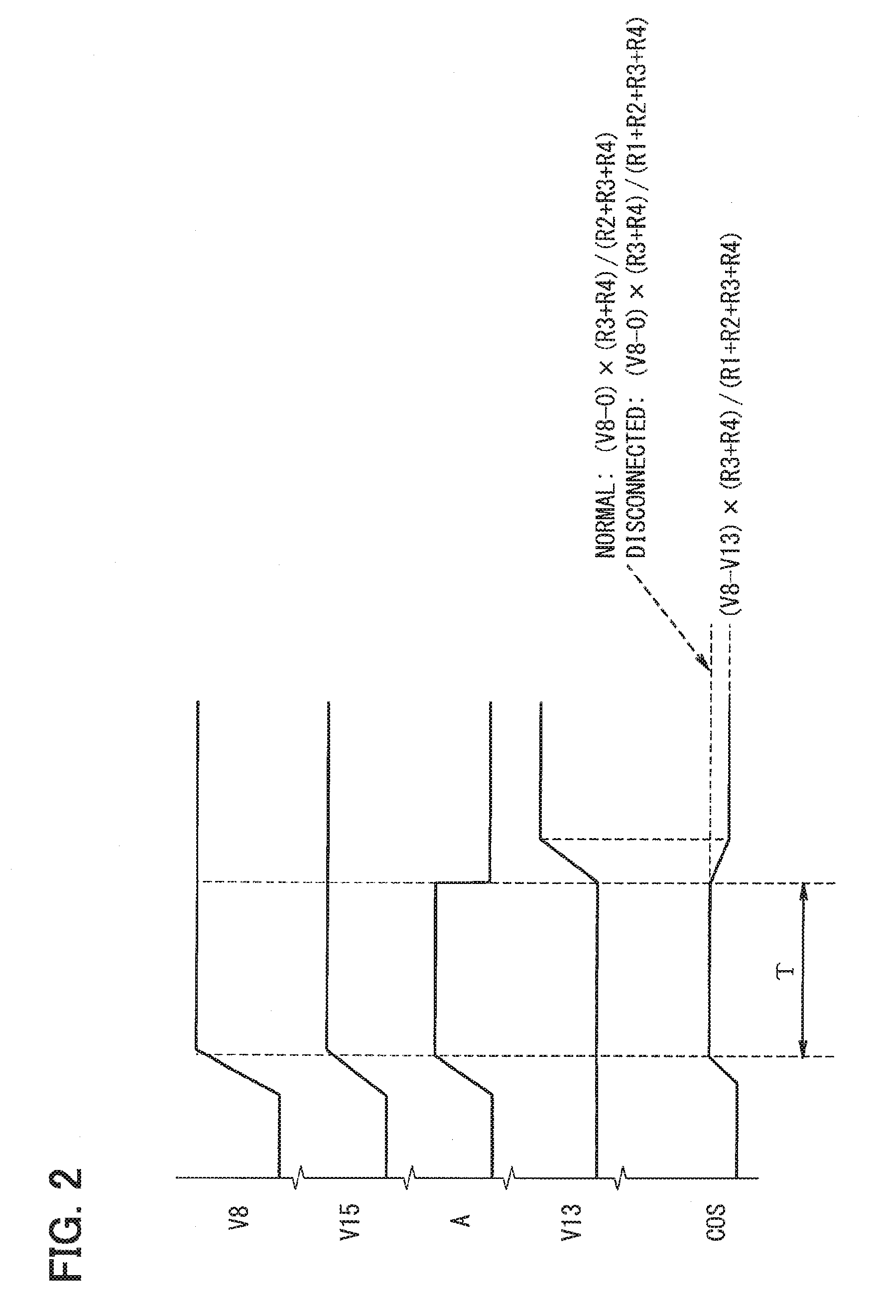
[0051]In a third embodiment, as shown in FIG. 4, an ECU 31 includes an IC 32, which is provided with a current check part 33 in place of the comparison logic part 16. The current check part 33 includes current meters 34C, 34S and a checker 35. The current meters 34C and 34S correspond to first and second current detection circuits, respectively. Input terminals of the current meter 34C are connected to both ends of the resistor element R3, respectively. Input terminals of the current meter 34S are connected to both ends of the resistor elements R7, respectively. The current meters 34C and 34S convert currents flowing in the resistor elements R3 and R7 into voltages, respectively, and output voltage signals to the checker 35.
[0052]In a case of the following signal input state (I) or (II), the checker outputs the DIAG signal to the microcomputer 30.[0053](I) Input from the current meter 34C: MAX current, and[0054]input from the current meter 34S: V15 / (R5+R6+R7+R8)[0055](II) Input from...
PUM
 Abstract
Description
Claims
Application Information