Touch panel and touch display device

a touch display device and touch technology, applied in the field of touch technology, can solve the problems of failure of touch electrode detection methods, unfavorable user experience, and inability to detect failure touch electrodes, so as to reduce anomalies, save pin resources, and reduce product defect rates

Inactive Publication Date: 2016-12-01
TCL CHINA STAR OPTOELECTRONICS TECH CO LTD
View PDF5 Cites 14 Cited by
  • Summary
  • Abstract
  • Description
  • Claims
  • Application Information

AI Technical Summary

Benefits of technology

[0005]The present invention provides a touch panel and touch display device mainly for solving the problem which solves the open circuit being between the touch electrodes and the controller efficiently. The present invention reduces the defective rate and also enhances the life time of the touch panel.
[0019]The advantages of the present invention are: comparing with the convention technology, the touch electrodes of the touch panel of the present invention respectively connect to the controller by at least two wires. Even though the single wire appears an open circuit or other anomalies, the electric connection between the touch electrode and the controller is still achieved by the other wire. The present invention reduces the anomalies resulting from the wire, such as an open circuit, to reduce the product defect rate and to save the pin resource of the controller. Moreover, the product life time can be also prolonged by using two wires for the electric connection further to save the cost for the users.

Problems solved by technology

In the exposure technology, the dust, foreign matter some particles or the large amount of static electricity causes the open circuit to result in the touch electrode being failure because of the open circuit in the single line.
Moreover, there is not any detection method for the fail touch electrode.
It brings the hidden worry to the user undoubtedly.

Method used


Image

  • Touch panel and touch display device
  • Touch panel and touch display device
  • Touch panel and touch display device

Examples


Embodiment Construction

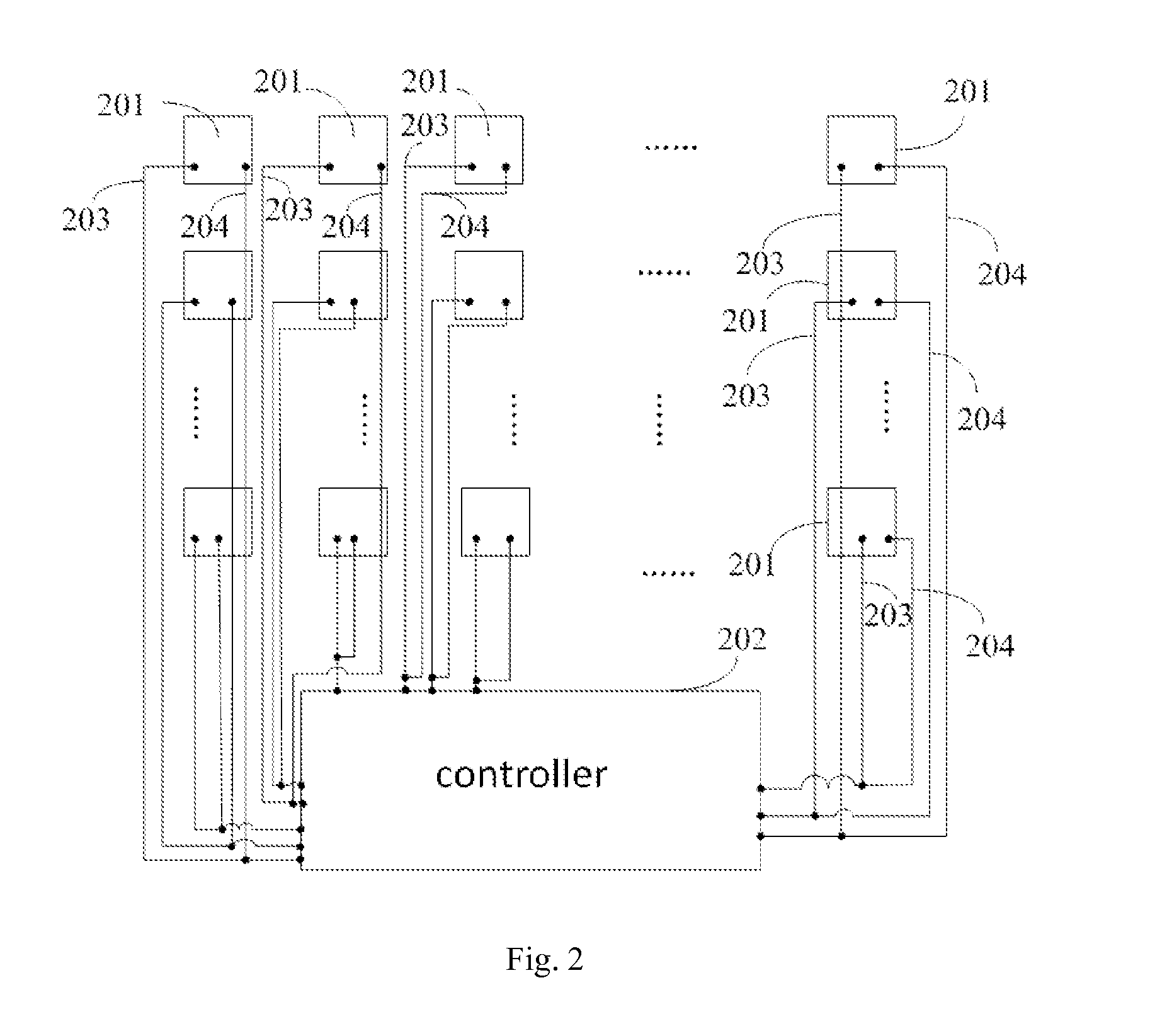
[0025]Please refer to FIG. 2 which is the structural diagram based on one embodiment of the touch panel of the present invention. The touch panel based on the embodiment of the present invention is an in-cell self-capacitance touch panel. In this embodiment, the touch panel comprises a plurality of the touch electrodes 201 arranged in a matrix and the controller 202. In this embodiment, the touch electrodes 201 are nano indium tin metal oxide (ITO) electrodes.

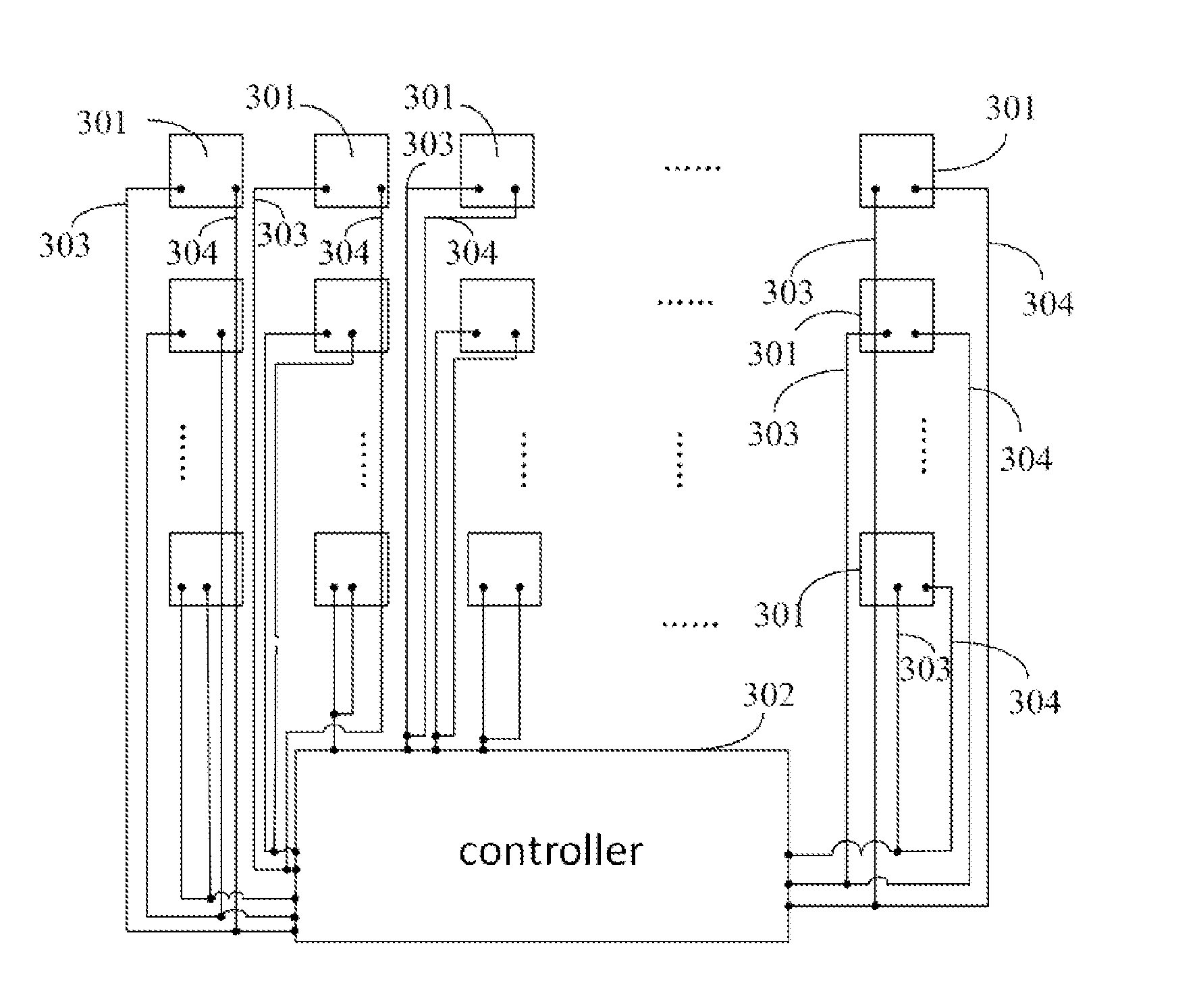
[0026]Where, at least the two wires electrically connecting between each of the touch electrodes 201 and the controller 202 are in one layer. As shown in FIG. 2, in the embodiment, each of the touch electrodes 201 connects to the controller 202 through the two wires 203 and 204.

[0027]In order to simplify the touch panel, and clarify the circuit, in the preferred embodiment, the wires 203 and 204 are respectively disposed in the different layers of the circuit board where the touch electrodes are arranged. For example, if the ci...


PUM

PropertyMeasurementUnit
capacitanceaaaaaaaaaa
transparent conductiveaaaaaaaaaa
self-capacitanceaaaaaaaaaa

Abstract

A touch panel and a touch display device are disclosed. The touch panel comprises a controller and a plurality of the touch electrodes arranged in a matrix, and each of the touch electrodes connects to a pin of the controller by using at least two wires. Through the above mentioned way, the present invention solves the open circuit issue between the touch electrode and the controller, reduces the defective rate and improves the life time of the touch panel.

Description

FIELD OF THE INVENTION[0001]The present invention relates to touch technology field; in particular to a touch panel and touch display device.BACKGROUND OF THE INVENTION[0002]Touch screens are also called as touch panels, which is a sensor type liquid crystal display device and can receive the input signal from contacting such as finger touching. When touching a graphical buttons, the tactile feedback system on the display makes sure of the action location of the touch according to the pre-set driving scan method. Further, to touch the graphical button is accurately to make sure the order type. Comparing with the conventional technology of the mechanical button panel, the touch panel is more convenient so it is wildly applied.[0003]There are many kinds of the touch panels wildly used, such as a vector pressure sensor touch screen, an infrared grid touch screen, a surface acoustic touch screen and a resistive touch screen. However, in the conventional technology, the capacitance type ...

Claims


Application Information

Patent Timeline
Patent Type & Authority Applications(United States)
IPC IPC(8): G06F3/041G02F1/1333G06F3/044
CPCG06F3/0416G06F3/044G06F2203/04103G02F1/13338G06F3/0412G06F3/04164G06F3/0443G06F3/041
Inventor LONG, CHONGSHEN, ZHIYUANSONG, TAO
Owner TCL CHINA STAR OPTOELECTRONICS TECH CO LTD
Why Eureka
Try Eureka