Package structure

Active Publication Date: 2016-12-01
DELTA ELECTRONICS SHANGHAI CO LTD
View PDF4 Cites 3 Cited by
  • Summary
  • Abstract
  • Description
  • Claims
  • Application Information

AI Technical Summary

Benefits of technology

The present invention provides a package structure with an elastomer to protect the substrate, wire, and electronic component from damage caused by pressure from the strut. This makes the fabricating process easier, as it is not necessary to precisely machine the strut. The technical effect of this invention is to minimize the risk of damage to the package and facilitate its fabrication.

Problems solved by technology

Under this circumstance, it is difficult to fabricate the package structure 1.
However, since the rigid struts are made of a rigid material and the structural strengths of the bonding wires and the electronic components are weak, the bonding wires or the electronic components are possibly damaged by the rigid struts.
Under this circumstance, the power module cannot be easily fabricated.

Method used


Image

  • Package structure
  • Package structure
  • Package structure

Examples


first embodiment

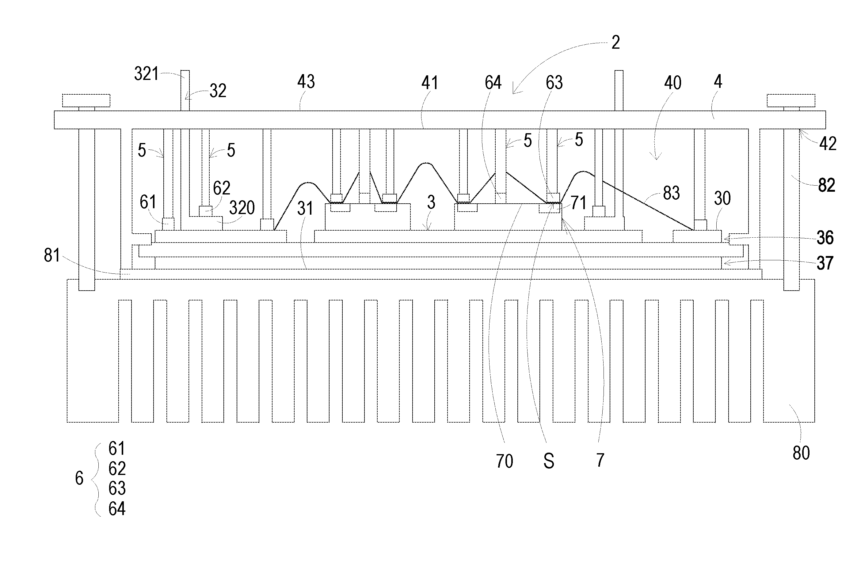
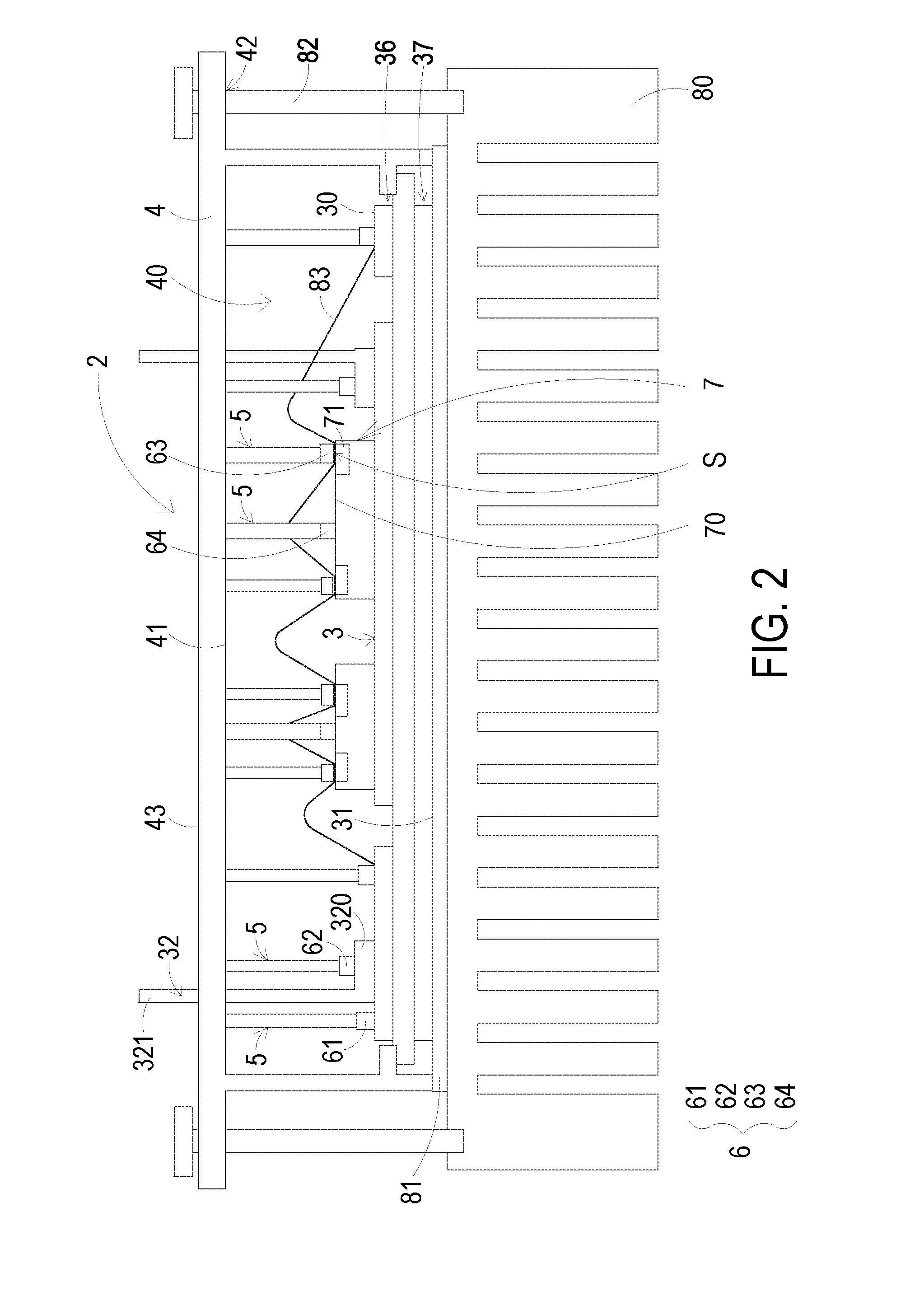
[0022]FIG. 2 schematically illustrates a package structure according to the present invention. As shown in FIG. 2, the package structure 2 comprises a substrate 3, a housing 4, at least one strut 5 and at least one elastomer 6. The substrate 3 has a first surface 30 and a second surface 31. At least one electronic component 7 is disposed on the first surface 30 of the substrate 3. The housing 4 is disposed on the first surface 30 of the substrate 3 for covering the first surface 30 of the substrate 3. Moreover, the housing 4 has an accommodation space 40 for accommodating the electronic component 7.

[0023]A first end of the strut 5 is disposed on an inner surface 41 of the housing 4. A second end of the strut 5 extends toward the first surface 30 of the substrate 3. Preferably but not exclusively, the elastic modulus of the elastomer 6 is lower than 1000 MPa. Moreover, the elastomer 6 is arranged between the substrate 3 and the strut 5. The elastomer 6 is configured to receive a pres...

second embodiment

[0039]FIG. 5 schematically illustrates a portion of a package structure according to the present invention. In this embodiment, the top surface and the bottom surface of the elastomer 6 are in contact with the objects of different materials. For providing better elastic properties, the elastomer 6 comprises a first elastic part 65 and a second elastic part 66. The first elastic part 65 is located over the second elastic part 66. The first elastic part 65 and the second elastic part 66 of the elastomer 6 have different elastic modulus. Moreover, as shown in FIG. 5, the second ends of plural struts 5 are in contact with the same elastomer 6.

[0040]FIG. 6A schematically illustrates a portion of a package structure according to a third embodiment of the present invention. FIG. 6B schematically illustrates the relationship between an elastomer and a substrate of the package structure according to the third embodiment of the present invention. FIG. 6C schematically illustrates the relation...

fourth embodiment

[0041]FIG. 7 schematically illustrates a portion of a package structure according to the present invention. As shown in FIG. 7, an insulation trench 34 is formed in the first conductive layer 36 of the substrate 3 by an etching process. By the insulation trench 34, the first conductive layer 36 is divided into plural conductive parts 35, and the plural conductive parts 35 are isolated from each other. Each of the conductive parts 35 is contacted with a conductive terminal (not shown) of the corresponding electronic component. Moreover, the elastomer 6 is accommodated within the insulation trench 34. For maintaining the isolation between the plural conductive parts 35, the elastomer 6 is made of an insulation material. Moreover, the strut 5 is partially accommodated within the insulation trench 34 and contacts with the elastomer 6. Since the elastomer 6 is accommodated within the insulation trench 34, the layout area of the first surface 30 of the substrate 3 is not adversely affecte...


PUM


Abstract

A package structure includes a substrate, at least one electronic component, a housing and at least one strut. The at least one electronic component is disposed on a first surface of the substrate. The housing covers the first surface of the substrate. The housing has an accommodation space. The at least one electronic component is accommodated within the accommodation space. The at least one strut is protruded from an inner surface of the housing and extended toward the accommodation space. The at least one elastomer is arranged between the corresponding strut and the substrate.

Description

FIELD OF THE INVENTION[0001]The present invention relates to a package structure, particularly to a package structure with elastomer, which can receive pressure from struts and transfer it to substrate.BACKGROUND OF THE INVENTION[0002]Recently, the general trends in designing electronic devices towards high density, high performance, small size, light weight and portability. Moreover, with the increasing development of electronic industries, the electronic devices are gradually modularized. Electronic components (e.g. active components and passive components) are integrated into a power module, then install the power module on a motherboard or a system circuit board.[0003]FIG. 1 schematically illustrates a package structure of a conventional power module. As shown in FIG. 1, the package structure 1 comprises a substrate 10, plural pins 11 and a housing 12. A process of fabricating the package structure 1 will be illustrated as follows. Firstly, active components (not shown), passive...

Claims


Application Information

Patent Timeline
IPC IPC(8): H01L23/24H01L23/04
CPCH01L23/041H01L23/24H01L2224/48139H01L23/4006H01L24/32H01L24/48H01L24/73H01L25/072H01L2224/04042H01L2224/32225H01L2224/48091H01L2224/48227H01L2224/73265H01L2224/8592H01L2924/1305H01L2924/19043H01L2924/19105H01L23/053H01L23/16H01L23/3735H01L23/49811H01L2924/00014H01L2924/00012H01L2224/45099H01L24/29
Inventor WAN, ZHENGFENWANG, TAOZHAO, ZHENQINGCHENG, WEIXU, HAIBIN
Owner DELTA ELECTRONICS SHANGHAI CO LTD
Why Eureka
Try Eureka