Organic electroluminescence module, smart device, and illumination device
Active Publication Date: 2016-12-15
KONICA MINOLTA INC
View PDF0 Cites 10 Cited by
Summary
Abstract
Description
Claims
Application Information
AI Technical Summary
This helps you quickly interpret patents by identifying the three key elements:
Problems solved by technology
Method used
Benefits of technology
Benefits of technology
The present invention provides an organic electroluminescent device that includes an electrode having both light-emitting and touch sensing functions. This reduces the size and thickness of the device and simplifies the production steps. The invention further includes an organic electroluminescent module with a specific controlling circuit that can make a significant contribution to the development of smaller and thinner devices. Additionally, the invention provides a smart device and an illumination device that utilize the organic electroluminescent module.
Problems solved by technology
Such a structure inevitably has a large thickness due to increased components and thus its use is restricted.
In use of such an assembly, a device for detecting the touch, such as an FPC, should be additionally prepared, resulting in several disadvantages, such as increased costs, increased thicknesses of the devices, and increased production steps.
Method used
Image
Click on the blue label to locate the original text in one second.
Reading with bidirectional positioning of images and text.
Examples
embodiment 1
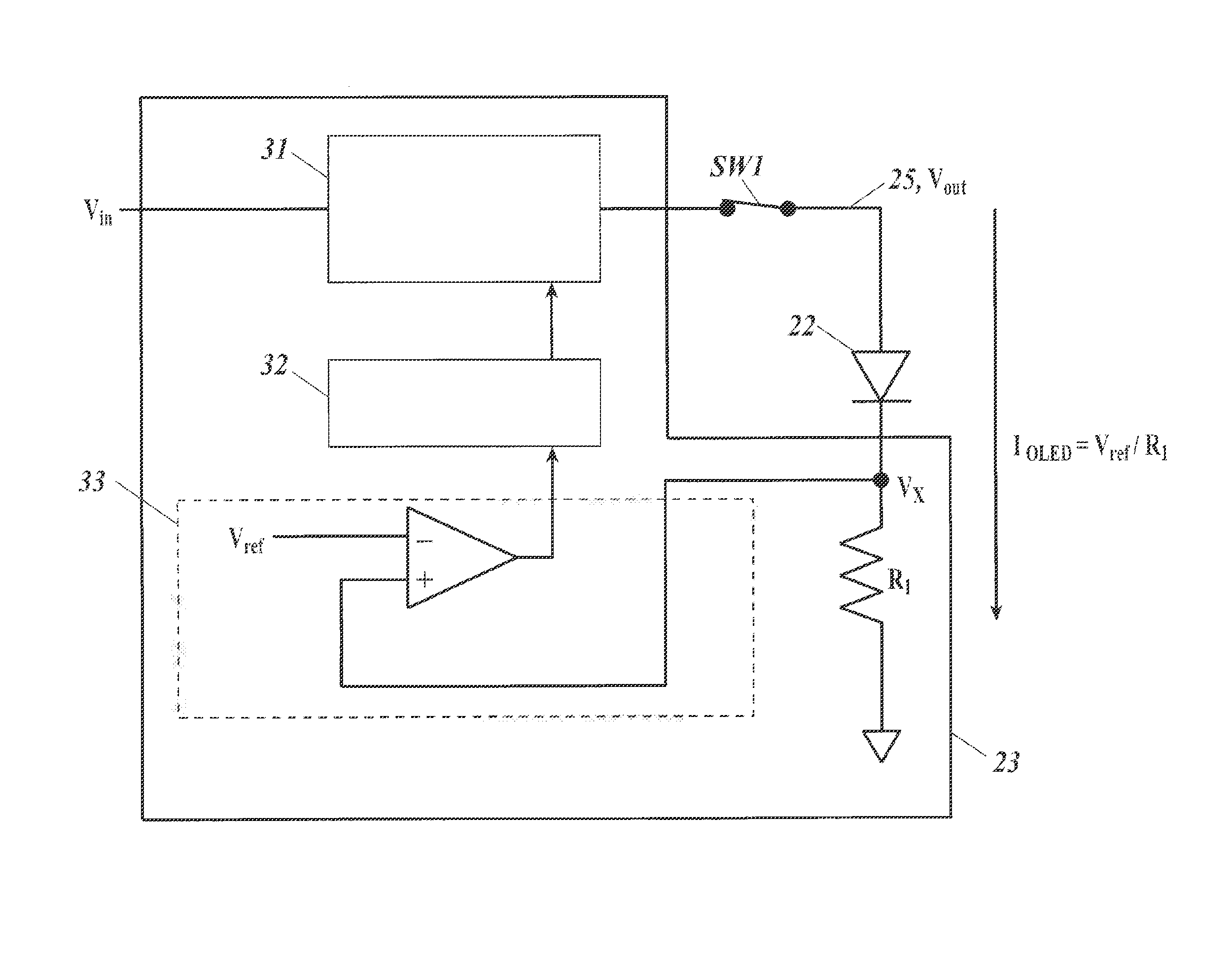
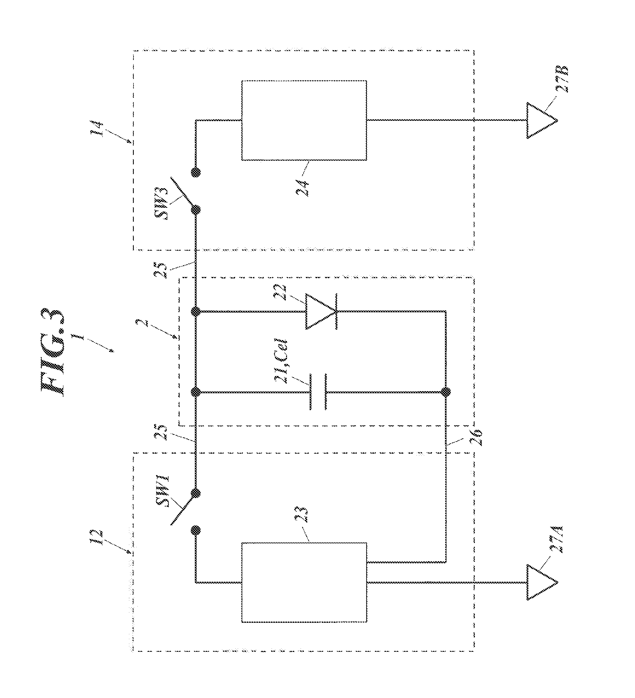
[0086]FIG. 3 illustrates a driving circuit for driving an organic EL module according to Embodiment 1.
[0087]In FIG. 3 illustrating a driving circuit for driving the organic EL module (1), the organic EL panel (2), which is illustrated on the middle of the drawing, includes an anode lead (25) connected to the anode (4A) (not shown) and a cathode lead (26) connected to the cathode (6) (not shown). An organic EL device (22) in the form of a diode and an interelectrode capacitorCel (21) are connected between the anode lead (25) and the cathode lead (26).
[0088]In the light-emitting device driving circuit unit (12), which is illustrated on the left of the drawing, the anode lead (25) extending from the anode (4A) (not shown) is connected to a light-emitting device driving circuit section (23) via a first switch (SW1), and the cathode lead (26) extending from the cathode (6) (not shown) is connected to the light-emitting device driving circuit section (23). The light-emitting device drivi...
embodiment 2
[0114]FIG. 9 is a driving circuit diagram of an organic EL module according to Embodiment 2 of the present invention.
[0115]The organic EL module (1) illustrated in FIG. 9 has the same drive circuit as that illustrated above in FIG. 3, except that a fourth switch (SW4) is provided between the anode lead (25) and the cathode lead (26) for short circuit.
[0116]The light-emitting device driving circuit section (23) may include the first switch (SW1) therein. The touch sensing circuit section (24) may include the third switch (SW3) therein.
[0117]FIG. 10 is a timing chart (pattern 3) illustrating an exemplary emission term and sensing term in Embodiment 2.
[0118]In contrast to the timing chart illustrated in FIG. 5, the first switch (SW1) in the timing chart illustrated in FIG. 10 including the fourth switch (SW4) is turned on throughout the emission term (LT) to activate the OLED, and then the first switch (SW1) is turned off while the third and fourth switches (SW3 and SW4) are being turn...
embodiment 3
[0123]FIG. 13 is a driving circuit diagram of an organic EL module according to Embodiment 3.
[0124]With reference to FIG. 13, the light-emitting device driving circuit unit (12) does not have the first switch (SW1). In this module, the organic electroluminescent panel continuously emits light, and the touch sensing term periodically occurs under the control of the touch sensing circuit section.
[0125]With reference to FIG. 13, the light-emitting device driving circuit unit (12) has no switch, and thus the circuit is always closed (“ON” state), resulting in continuous emission of light from the organic EL device (22). The light-emitting device driving circuit section (23) is connected to the independent ground (27A).
[0126]In contrast, in the touch sensing circuit unit (14) illustrated at the right side, the anode lead (25) extracted from the anode functioning as a touch sensing electrode is connected to the touch sensing circuit section (24) via the third switch (SW3). This touch sens...
PUM
Abstract
An object of the present invention is to provide an organic EL device that includes an electrode having a light-emitting function and a touch sensing function, an organic electroluminescent module that includes a specific controlling circuit and can contribute to reduction in sizes and thickness and simplified production steps of the device, and a smart device and an illumination device each including the organic electroluminescent module. The organic electroluminescent module of the present invention has a touch sensing function and includes a touch sensing circuit unit and a light-emitting device driving circuit unit including a light-emitting device driving circuit section for driving an organic electroluminescent panel. The organic electroluminescent panel includes paired opposite electrodes therein. The paired electrodes are connected to the light-emitting device driving circuit unit, and one of the paired electrodes is a touch sensing electrode that is connected to the touch sensing circuit unit. The touch sensing circuit unit and the light-emitting device driving circuit unit are connected to independent grounds.
Description
TECHNICAL FIELD[0001]The present invention relates an organic electroluminescent module having a touch sensing function, and a smart device and an illumination device provided with the module.BACKGROUND ART[0002]Examples of traditional flat light sources include light emitting diodes (LEDs) provided with light guiding plates, and organic light emitting diodes (OLEDs) or organic electroluminescent devices (OLEDs).[0003]Smart devices, such as smart phones and tablets, have gotten exponential increased sales on a world scale from around 2008. These smart devices are provided with a keyboard having a flat face in view of user-friendliness. For example, the keyboard corresponds to the icon region including common functional key buttons provided at the bottom of a smart device. One example combination of the common functional key buttons consists, for example, of “Home” (indicated by a square mark), “Return” (indicated by an arrow mark), and “Search” (indicated by a loupe mark).[0004]In o...
Claims
Application Information
Patent Timeline
Application Date:The date an application was filed.
Publication Date:The date a patent or application was officially published.
First Publication Date:The earliest publication date of a patent with the same application number.
Issue Date:Publication date of the patent grant document.
PCT Entry Date:The Entry date of PCT National Phase.
Estimated Expiry Date:The statutory expiry date of a patent right according to the Patent Law, and it is the longest term of protection that the patent right can achieve without the termination of the patent right due to other reasons(Term extension factor has been taken into account ).
Invalid Date:Actual expiry date is based on effective date or publication date of legal transaction data of invalid patent.

