Production method for electronic component and pressure-sensitive adhesive sheet to be used in the production method

Inactive Publication Date: 2014-02-13
NITTO DENKO CORP
View PDF0 Cites 21 Cited by
  • Summary
  • Abstract
  • Description
  • Claims
  • Application Information

AI Technical Summary

Benefits of technology

[0024]According to the present invention, through use of a pressure-sensitive adhesive sheet having a predetermined configuration, a dielectric protective layer can be formed easily on an electrode surface of a chip-shaped electronic component. The dielectric protective layer can serve as an insulating layer in formation of the above-mentioned redistribution layer, which leads to simplification of the step of forming a redistribution layer in a production method for a chip-shaped electronic component. Further, in the present invent

Problems solved by technology

In this case, when processes such as redistribution are performed on the wafer in a collective manner without discriminating defective products from non-defective products, a process performed with respect to the defective products becomes waste, resulting in an increase in production cost of the non-defective products which can be shipped.
Further, the WL-CSP requires many complicated processing steps.
However, a thickness of a semiconductor chip is becoming small, and hence with only a thickness of such dielectric protective layer, it is highly probable that the semiconductor chi

Method used


Image

  • Production method for electronic component and pressure-sensitive adhesive sheet to be used in the production method
  • Production method for electronic component and pressure-sensitive adhesive sheet to be used in the production method
  • Production method for electronic component and pressure-sensitive adhesive sheet to be used in the production method

Examples


Example

A. Pressure-Sensitive Adhesive Sheet

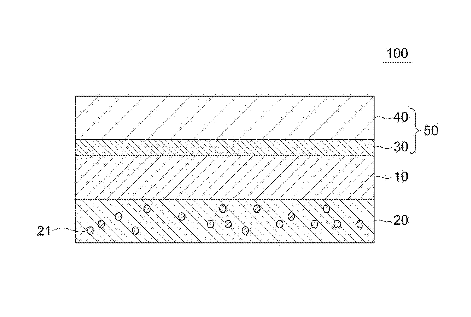
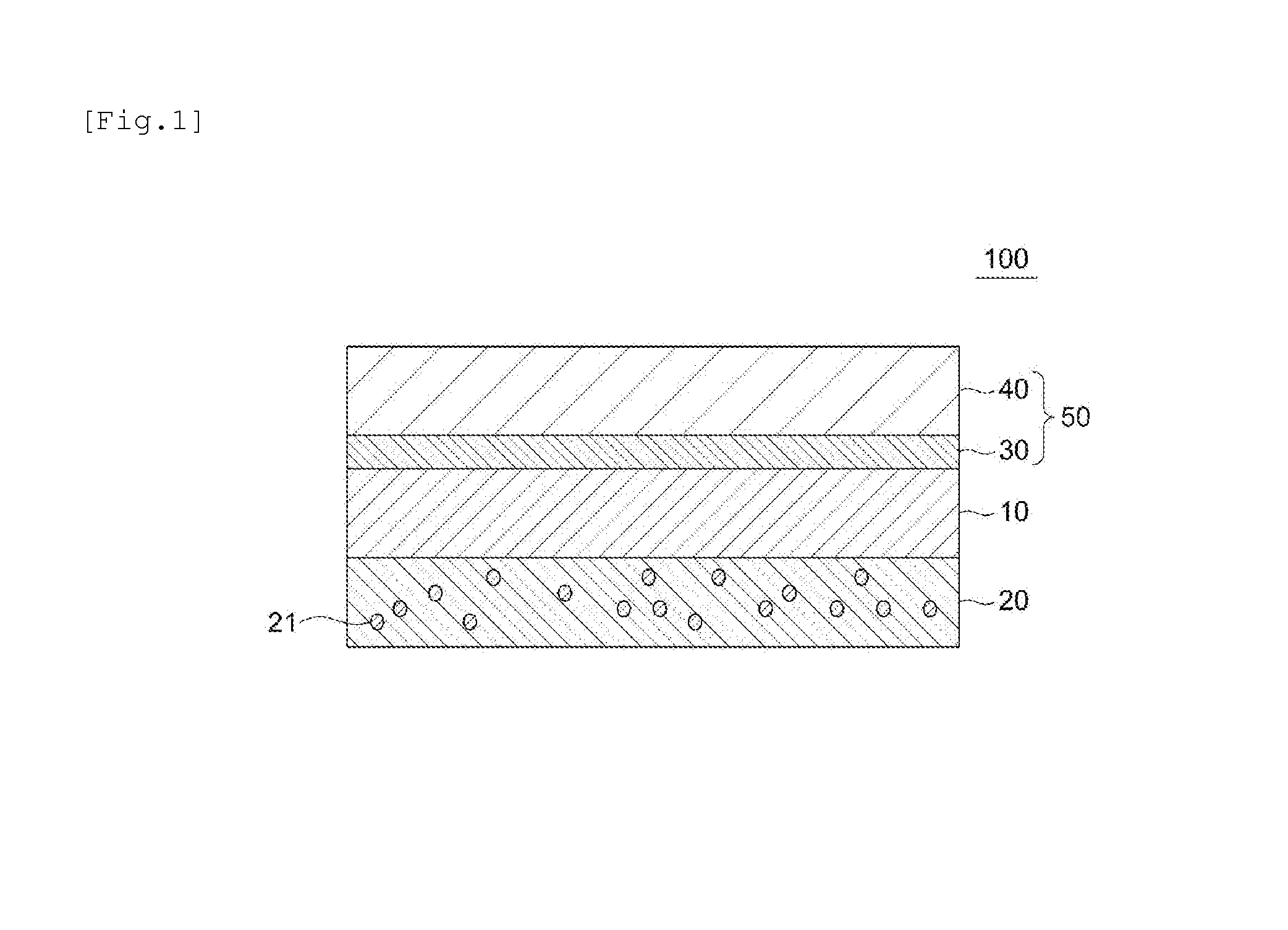
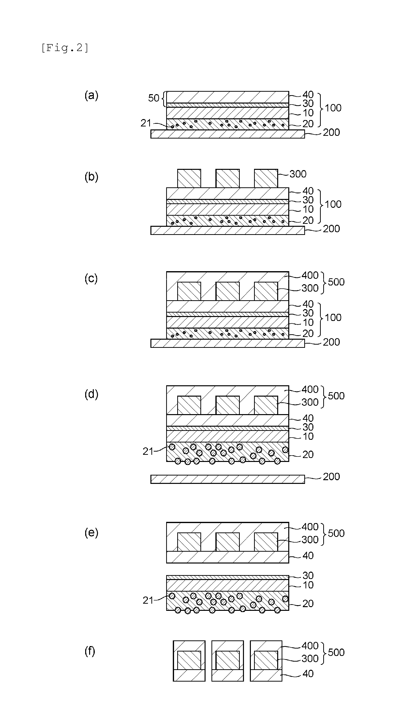
[0027]In one aspect, the present invention provides a pressure-sensitive adhesive sheet. The pressure-sensitive adhesive sheet of the present invention includes a base, a thermally expandable pressure-sensitive adhesive layer containing thermally expandable microspheres provided on one surface of the base, and a dielectric layer including a weak pressure-sensitive adhesive layer and an adhesive layer provided on the other surface of the base in this order from the base side. The pressure-sensitive adhesive sheet of the present invention is suitably used in a production method for an electronic component. The production method typically includes: attaching the pressure-sensitive adhesive sheet of the present invention to a substrate so that the thermally expandable pressure-sensitive adhesive layer is placed on the substrate side; attaching and fixing a plurality of chip-shaped electronic components to a surface of the pressure-sensitive adhesive s...


PUM

PropertyMeasurementUnit
Temperatureaaaaaaaaaa
Energyaaaaaaaaaa

Abstract

A simplified production method for a chip-shaped electronic component such as a semiconductor chip is provided.
The production method of the present invention includes: attaching a pressure-sensitive adhesive sheet to a substrate, the pressure-sensitive adhesive sheet including a base, a thermally expandable pressure-sensitive adhesive layer containing thermally expandable microspheres provided on one surface of the base, and a dielectric layer including a weak pressure-sensitive adhesive layer and an adhesive layer provided on another surface of the base in this order from a side of the base, so that the thermally expandable pressure-sensitive adhesive layer is placed on a side of the substrate; attaching and fixing a plurality of chip-shaped electronic components to a surface of the pressure-sensitive adhesive sheet on a side of the adhesive layer so that electrode surfaces of the plurality of chip-shaped electronic components are placed on the side of the adhesive layer; covering an entire surface of the plurality of chip-shaped electronic components excluding fixed surfaces with a protective substance to obtain an encapsulated body including the plurality of chip-shaped electronic components; subjecting the pressure-sensitive adhesive sheet to heating treatment to cause the thermally expandable microspheres in the thermally expandable pressure-sensitive adhesive layer to expand to decrease an adhesion of the thermally expandable pressure-sensitive adhesive layer and peeling the thermally expandable pressure-sensitive adhesive layer from the substrate; peeling the weak pressure-sensitive adhesive layer from the adhesive layer to obtain a laminate of the adhesive layer and the encapsulated body; and cutting the laminate between the plurality of chip-shaped electronic components to separate individual chip-shaped electronic components.

Description

TECHNICAL FIELD[0001]The present invention relates to a production method for an electronic component, and to a pressure-sensitive adhesive sheet to be used in the production method.BACKGROUND ART[0002]In production of a semiconductor chip, a package system called a wafer level chip size package (WL-CSP) in which packaging is performed in a wafer state for the purpose of high-density packaging is drawing attention. According to the WL-CSP, a wafer is subjected to dicing after redistribution, formation of terminals, and the like are performed on the wafer, and hence a semiconductor package reduced in size almost to a chip size can be obtained.[0003]In this connection, a plurality of circuit patterns formed on one wafer may include defective products. In this case, when processes such as redistribution are performed on the wafer in a collective manner without discriminating defective products from non-defective products, a process performed with respect to the defective products becom...

Claims


Application Information

Patent Timeline
IPC IPC(8): C09J7/02C09J7/38
CPCC09J7/0207C09J7/38H01L21/568H01L23/293H01L23/3114H01L21/565H01L2924/0002C09J2203/326C09J2301/1242C09J2301/208C09J2301/412H01L21/68H01L21/561H01L24/97Y10T428/254H01L2924/00012C09J11/00C09J201/00H01L21/30H01L21/50
Inventor HIRAYAMA, TAKAMASASHIMOKAWA, DAISUKE
Owner NITTO DENKO CORP
Why Eureka
Try Eureka