Array substrate and method of repairing broken lines for the array substrate

a technology of array substrate and broken line, applied in the field of display skill, can solve the problems of inability to directly implement broken line repair, large thickness of organic layer, easy to break lines, etc., and achieve the effects of reducing the cost of laser energy consumption

Active Publication Date: 2016-12-15
SHENZHEN CHINA STAR OPTOELECTRONICS TECH CO LTD
View PDF0 Cites 6 Cited by
  • Summary
  • Abstract
  • Description
  • Claims
  • Application Information

AI Technical Summary

Benefits of technology

[0027]The benefits of the present invention are: in the array substrate and the method of repairing broken lines for the array substrate according to the present invention, by preserving the via on the organic layer corresponding to the cross point of the source-drain data line and the common electrode line, the aperture formed with the second passivation layer deposed in the via is employed to be the laser welding point as the source-drain data line is broken. After detecting the broken line position of the source-drain, the laser welding is implemented to the apertures at two ends of the broken line position to lap the source-drain data line with the closed ring of the common electrode line, and meanwhile, the connection lines at two sides of the closed ring of the common

Problems solved by technology

The broken line can easily happen in the manufacture process, it requires the laser to implement the operation of the broken line repair.
When the broken line defect happened to the data line, the thickness of the organic layer is larger, and the broken line repair cannot be directly im

Method used


Image

  • Array substrate and method of repairing broken lines for the array substrate
  • Array substrate and method of repairing broken lines for the array substrate
  • Array substrate and method of repairing broken lines for the array substrate

Examples


Embodiment Construction

[0035]For better explaining the technical solution and the effect of the present invention, the present invention will be further described in detail with the accompanying drawings and the specific embodiments.

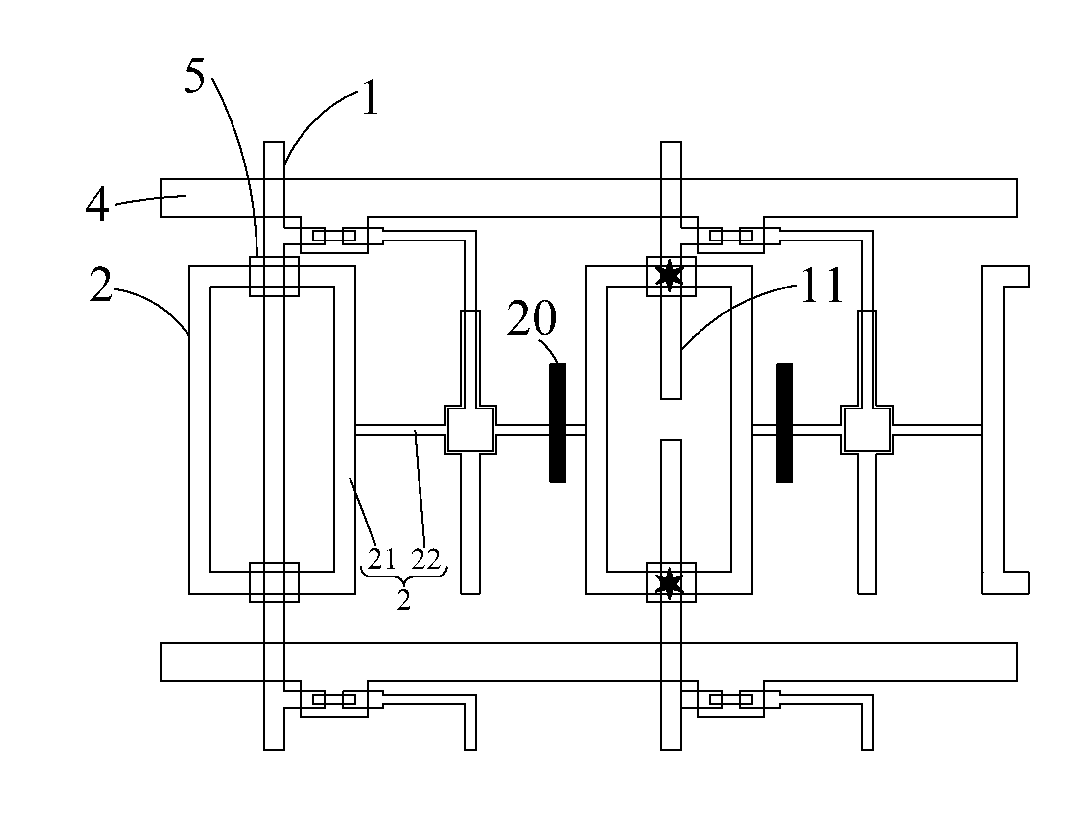
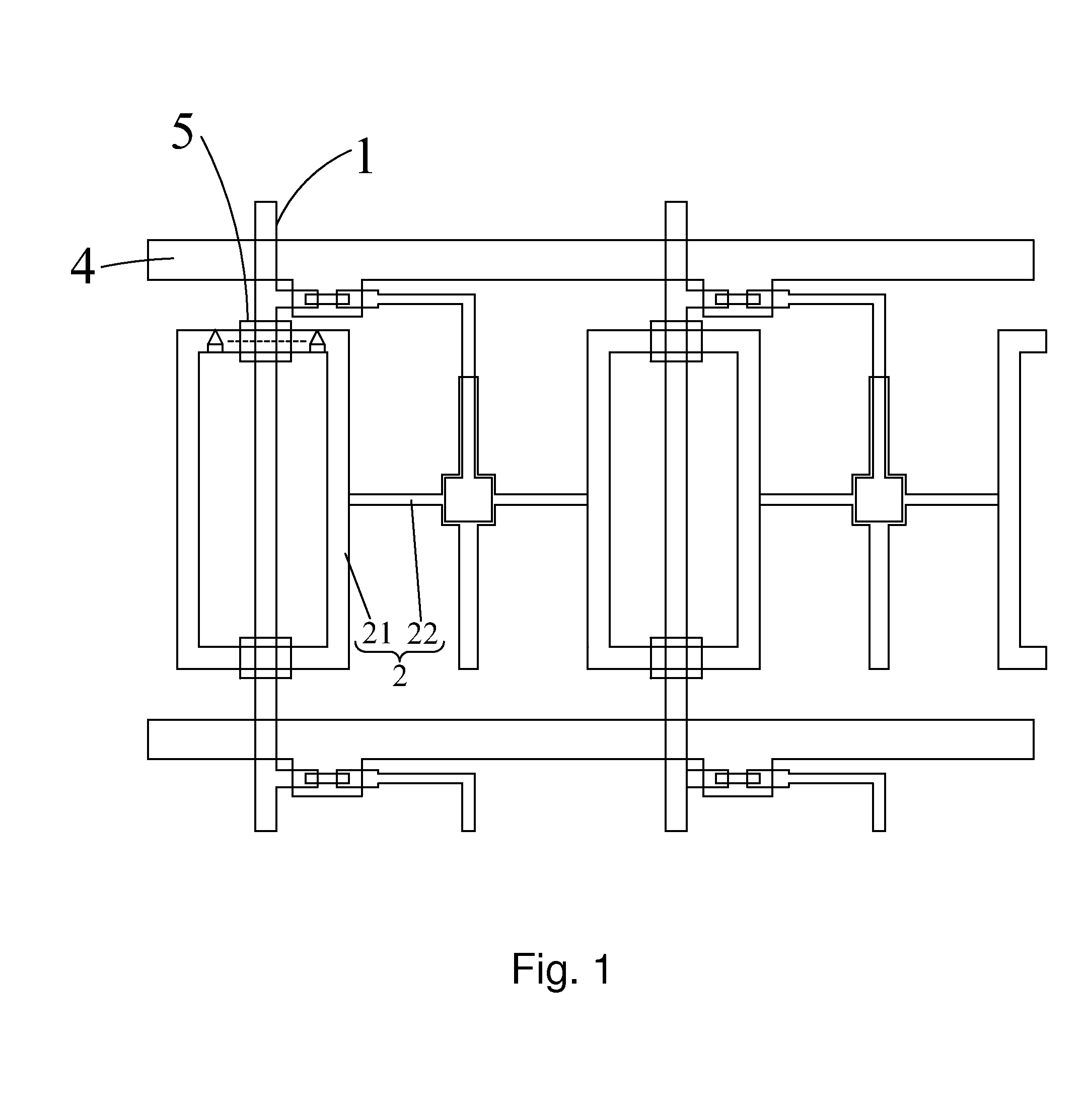
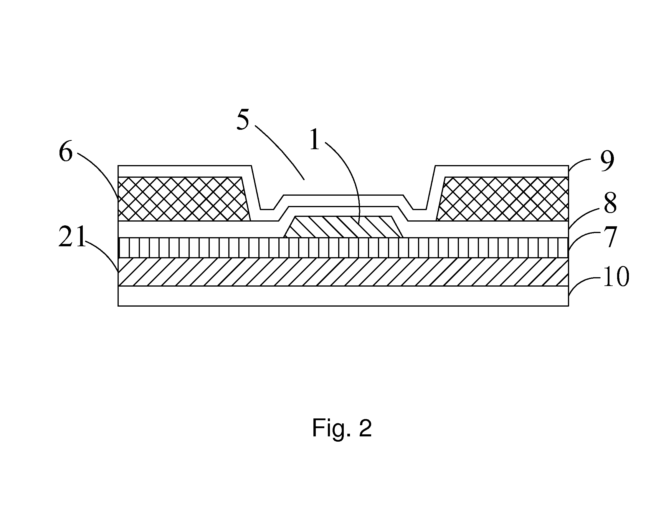
[0036]Please refer to FIG. 1 and FIG. 2. The present invention first provides an array substrate, comprising a substrate 10, a gate scan line 4 and a common electrode line 2 positioned on the substrate 10, a gate isolation layer 7 positioned on the gate scan line 4 and the common electrode line 2, a source-drain data line 1 positioned on the gate isolation layer 7, a first passivation layer 8 positioned on the source-drain data line 1, an organic layer 6 positioned on the first passivation layer 8 and a second passivation layer 9 positioned on the organic layer 6 and the first passivation layer 8;

[0037]Specifically, the common electrode line 2 comprises a plurality of closed rings 21 and a plurality of connection lines 22, and the plurality of closed rings 21 are connected tog...


PUM


Abstract

The present invention provides an array substrate and a method of repairing broken lines for the array substrate. By preserving the via on the organic layer corresponding to the cross point of the source-drain data line and the common electrode line, the aperture formed with the second passivation layer deposed in the via is employed to be the laser welding point as the source-drain data line is broken. After detecting the broken line position of the source-drain, the laser welding is implemented to the apertures at two ends of the broken line position to lap the source-drain data line with the closed ring of the common electrode line, and meanwhile, the connection lines at two sides of the closed ring of the common electrode line is cut with laser, and the closed ring of the common electrode line is employed to repair the broken line part of the source-drain data line.

Description

FIELD OF THE INVENTION[0001]The present invention relates to a display skill field, and more particularly to an array substrate and a method of repairing broken lines for the array substrate.BACKGROUND OF THE INVENTION[0002]With the development of display technology, the flat panel device, such as Liquid Crystal Display (LCD) possesses advantages of high image quality, power saving, thin body and wide application scope. Thus, it has been widely applied in various consumer electrical products, such as mobile phone, television, personal digital assistant, digital camera, notebook, laptop, and becomes the major display device.[0003]Most of the liquid crystal displays on the present market are back light type liquid crystal displays, which comprise a shell, a liquid crystal display panel located in the shell and a backlight module located in the shell. The liquid crystal display panel is a major component of the liquid crystal display. However, the liquid crystal display panel itself do...

Claims


Application Information

Patent Timeline
IPC IPC(8): G02F1/1362G02F1/1335H01L27/12G02F1/1333
CPCG02F1/136259G02F1/133345G02F1/133514G02F2001/136263H01L27/1248G02F2201/121G02F1/136286G02F1/136263G02F1/1343G02F1/1368
Inventor LI, SHAN
Owner SHENZHEN CHINA STAR OPTOELECTRONICS TECH CO LTD
Why Eureka
Try Eureka