Device of Chip Resistor with Terminal Electrodes

a terminal electrode and chip resistor technology, applied in the field of chip resistors, can solve the problems of affecting the final resistance of the resistor, increasing the cost of the front terminal electrode, and increasing the price of the resistor, so as to reduce the parasitic resistance effect of the resistor layer, improve the yield of electrical tests, and improve conductivity

Active Publication Date: 2016-12-22
NAT CHENG KUNG UNIV
View PDF0 Cites 6 Cited by
  • Summary
  • Abstract
  • Description
  • Claims
  • Application Information

AI Technical Summary

Benefits of technology

[0004]Another purpose of the present invention is to provide plated nickel having better conductivity than that of printed silver, where the plated nickel is directly connected to a low-resistance resistor layer for significantly reduce the parasitic resistance effect of the resistor layer; and the low-resistance resistor layer helps enhancing yield of electrical tests of resistor layers.
[0005]Another purpose of the present invention is to use printed silver on a front surface as a seed layer for forming plated nickel in post, where printed silver is not required for conducting the resistor layer; conductivity of front terminal electrode only has to suit the plated nickel; and not only a printed silver having a low silver content with low cost but also other low-cost metals having low conductivities can be used, which is advantageous for reducing the material cost of the chip resistor.

Problems solved by technology

Yet, the conductivity of the front terminal electrode must be much lower than the resistivity of the resistor layer to form an ohmic contact with the resistor layer; or else, parasitic resistance will affect the final resistance of the resistor.
However, the higher the solid content of silver, the more expensive the price.
As a result, the cost of the front terminal electrode is greatly increased.
In addition, for a low-resistance resistor, even through the front terminal electrode is made to have a lower resistance than that of the resistor layer, the final resistance of the entire resistor will still be affected to make a narrow-variation low-resistance resistor become hard to control.
Hence, the prior art does not fulfill all users' needs in actual use.

Method used


Image

  • Device of Chip Resistor with Terminal Electrodes
  • Device of Chip Resistor with Terminal Electrodes
  • Device of Chip Resistor with Terminal Electrodes

Examples


Embodiment Construction

[0012]The following description of the preferred embodiments is provided to understand the features and the structures of the present invention.

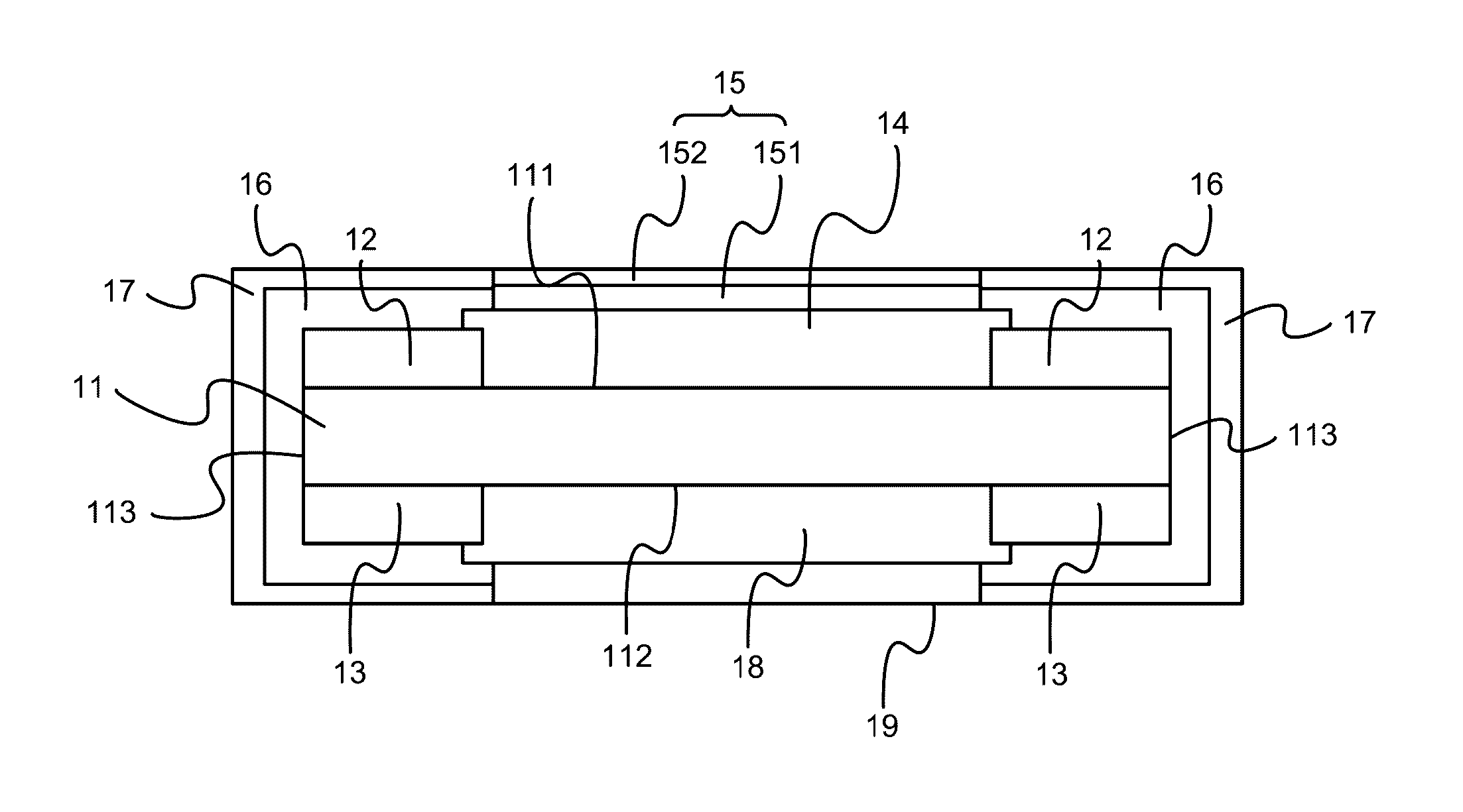
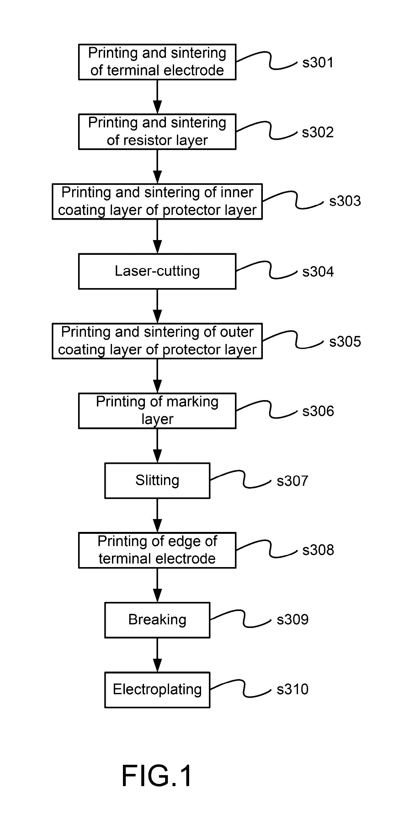
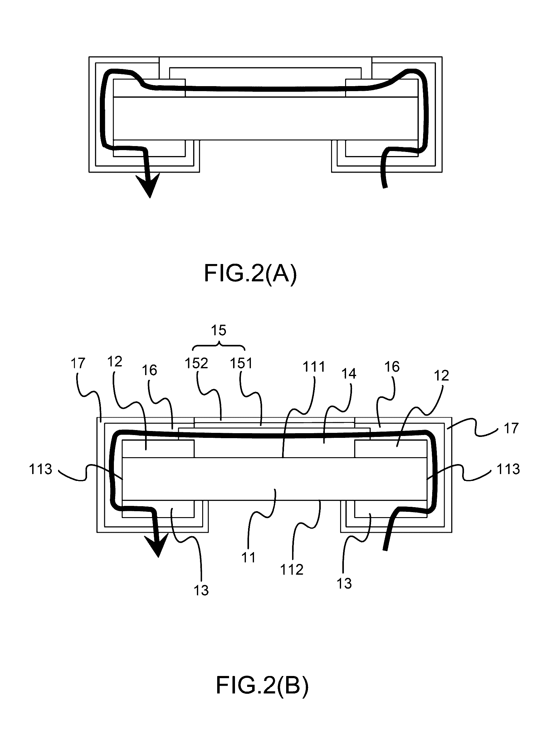
[0013]Please refer to FIG. 1˜FIG. 4, which are a flow view showing a producing process of a first preferred embodiment according to the present invention; a view showing comparison of current conduction paths for the present invention; a sectional view showing a second preferred embodiment; and a view showing comparison of resistance distributions. As shown in the figures, the present invention is a chip resistor device having terminal electrodes, where a first preferred embodiment comprises a substrate 11, two front terminal electrodes 12, two back terminal electrodes 13, a first resistor layer 14, a first protector layer 15 and two side terminal electrodes 16, as shown in FIG. 2(b).

[0014]The substrate 11 has a front surface 111, a back surface 112 and two side surfaces 113.

[0015]The front terminal electrodes 12 are formed on the front surf...


PUM


Abstract

A chip resistor having terminal electrodes is provided. In the chip resistor, a first protector layer has a size different from that of a first resistor layer. Thus, two ends of the first resistor layer are exposed to form new current conduction path. Original current conduction path having the same size of the protective layer and the resistor layer is thus replaced. Hence, resistance variation of the chip resistor is solved; yield of the chip resistor is increased; and, the material cost of the front terminal electrode is greatly reduced.

Description

TECHNICAL FIELD OF THE INVENTION[0001]The present invention relates to chip resistor; more particularly, relates to replacing an original current conduction path having the same size of a protective layer and a resistor layer by forming a new current conduction path having mutually different sizes of a protective layer and a resistor layer for solving resistance variation of chip resistor and further increasing yield of chip resistor while material cost of front terminal electrode is greatly reduced.DESCRIPTION OF THE RELATED ARTS[0002]Resistance of a chip resistor is mainly decided by the material and geometry of the resistor layer. After being conducted through front terminal electrodes, the chip resistor is connected to a printed circuit board (PCB) through electroplated nickel and tin. Basically, the terminal electrodes of the chip resistor can be divided into three parts, which are namely front terminal electrodes, back terminal electrodes and side terminal electrodes. Therein,...

Claims


Application Information

Patent Timeline
Patent Type & Authority Applications(United States)
IPC IPC(8): H01C1/14
CPCH01C1/146H01C1/14H01C1/028H01C1/148H01C7/003H01C17/02H01C17/281
Inventor LEE, WEN-HSI
Owner NAT CHENG KUNG UNIV
Why Eureka
Try Eureka