Multilayer thin-film back contact system for flexible photovoltaic devices on polymer substrates
- Summary
- Abstract
- Description
- Claims
- Application Information
AI Technical Summary
Benefits of technology
Problems solved by technology
Method used
Image

Examples
Embodiment Construction
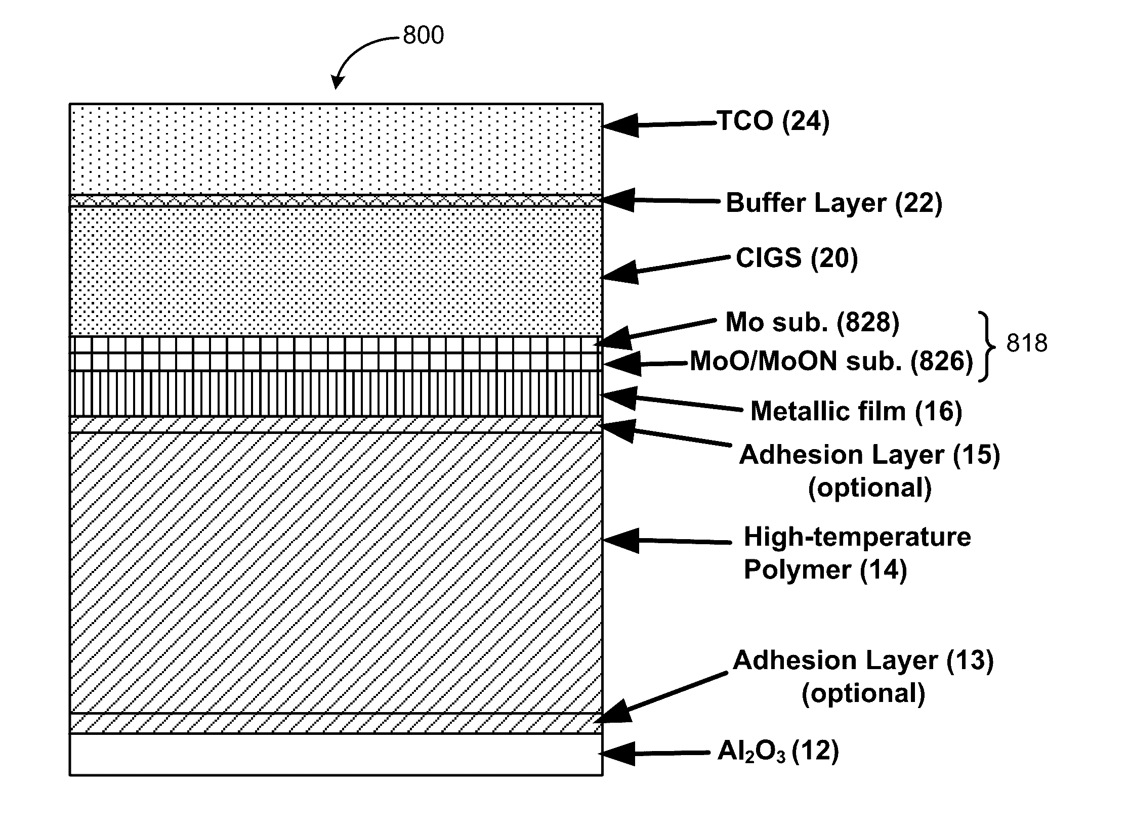
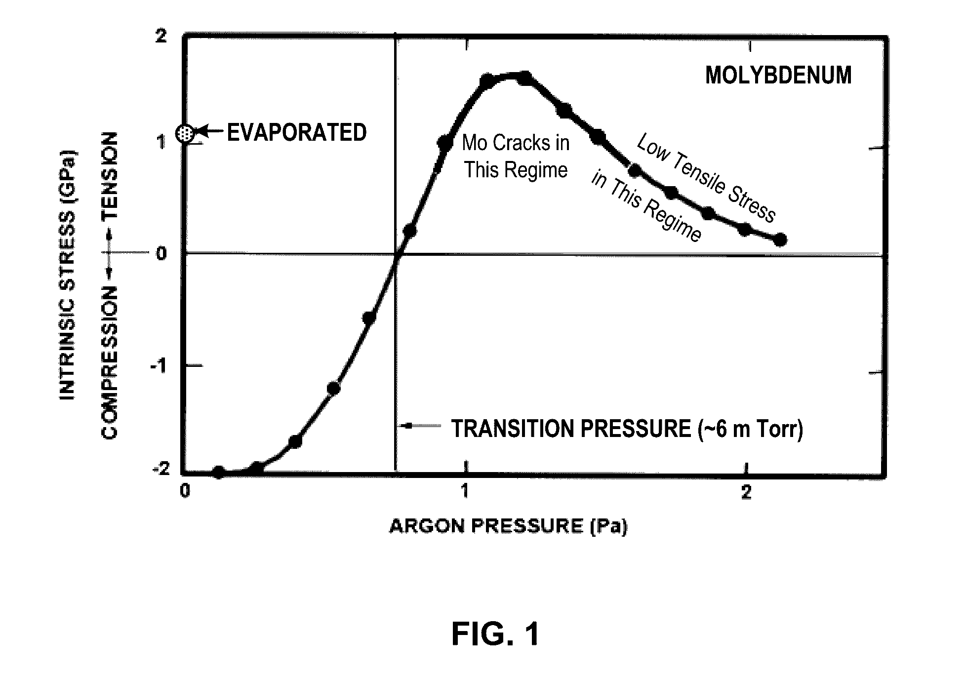
[0040]For CIGS devices, molybdenum (Mo) has been a common choice of material for a back contact, regardless of the substrate. While Mo can be deposited in a straightforward manner using DC sputtering or other thin film deposition methods, the wide range of stress states possible with sputtering can particularly complicate deposition onto flexible substrates, particularly those that do not exhibit significant stiffness, such as polymers. Unlike rigid substrates where the film stresses can readily be borne by the substrate, film stresses can have a significant impact upon the life, surface topology, and physical properties of flexible substrates, particularly substrates made from polymers. This class of substrates, while exhibiting excellent dielectric properties that allow monolithic integration, also typically exhibits high and inconsistent thermal expansion coefficient compared to the metals and semiconductors of the CIGS layer stack. Thus, there exist extrinsic stresses that combi...
PUM
 Abstract
Description
Claims
Application Information
 - R&D Engineer
- R&D Manager
- IP Professional
- Industry Leading Data Capabilities
- Powerful AI technology
- Patent DNA Extraction
Browse by: Latest US Patents, China's latest patents, Technical Efficacy Thesaurus, Application Domain, Technology Topic.
© 2024 PatSnap. All rights reserved.Legal|Privacy policy|Modern Slavery Act Transparency Statement|Sitemap