Insulated gate type semiconductor device

Active Publication Date: 2017-01-12
TOYOTA JIDOSHA KK
View PDF0 Cites 6 Cited by
  • Summary
  • Abstract
  • Description
  • Claims
  • Application Information

AI Technical Summary

Benefits of technology

The insulated gate type semiconductor device described in this patent text has a unique structure that allows for efficient depletion of the outer periphery region while also minimizing damage to the device during production and operation. The device includes a trench structure with multiple partition walls, which are designed to deform and absorb stress during production and operation, thereby preventing damage to the device. The narrow widths of the partition walls also facilitate the extension of the depletion layer from one trench to another, improving the device's withstand voltage.

Problems solved by technology

In each drift region present between two device portion bottom surface surrounding regions, depletion progresses from both sides, and therefore the drift region is easily depleted.
If the partition wall is thin, the partition wall may be deformed by the stress, whereby damage such as crack is likely to occur in the partition wall.

Method used


Image

  • Insulated gate type semiconductor device
  • Insulated gate type semiconductor device
  • Insulated gate type semiconductor device

Examples


first embodiment

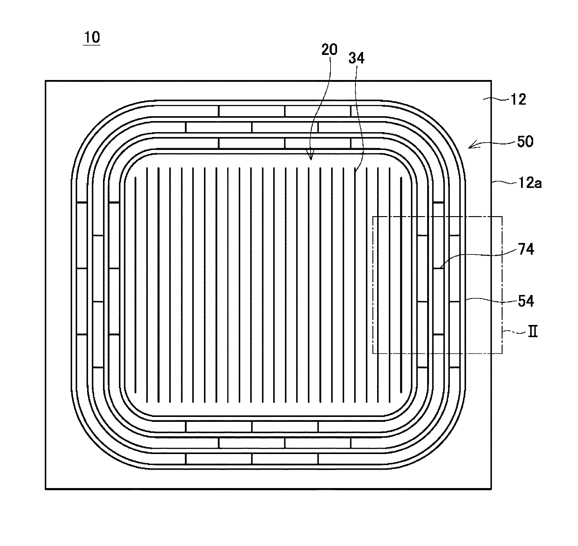
[0031]The semiconductor device 10 shown in FIGS. 1 and 2 has a semiconductor substrate 12 made of SiC. In FIGS. 1 and 2, an electrode, an insulating film, and the like on the semiconductor substrate 12 are not shown. The semiconductor substrate 12 has a cell region 20 and an outer periphery region 50. In the cell region 20, a MOSFET is formed. The outer periphery region 50 is a region between the cell region 20 and an end surface 12a of the semiconductor substrate 12.

[0032]As shown in FIG. 3, on a front surface of the semiconductor substrate 12, a front surface electrode 14 and an insulating layer 16 are formed. The insulating layer 16 covers the front surface of the semiconductor substrate 12 in the outer periphery region 50. The front surface electrode 14 is in contact with the semiconductor substrate 12 in the cell region 20. In other words, a region in which the front surface electrode 14 is in contact with the semiconductor substrate 12 is the cell region 20, and a region on an...

second embodiment

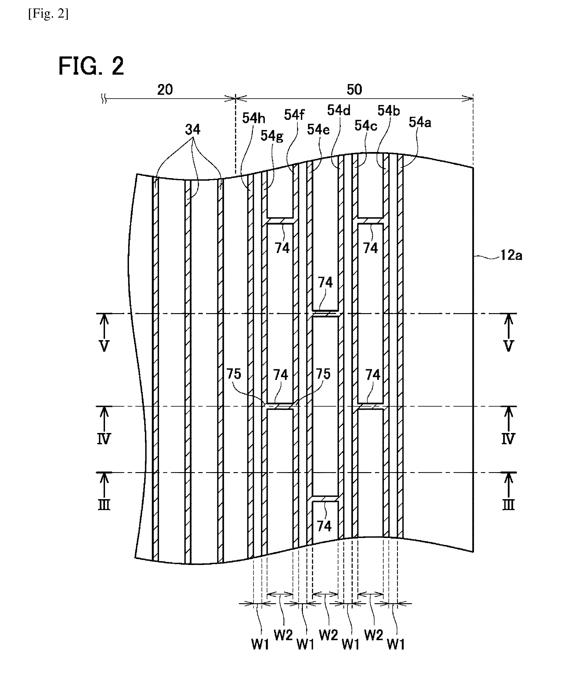
[0061]In a semiconductor device of the second embodiment, arrangement of the intervening trenches 74 is different from that in the first embodiment, but the other configuration is the same as that in the first embodiment. As shown in FIG. 2, in the first embodiment, the adjacent intervening trenches 74 are arranged in a staggered manner. On the other hand, in the semiconductor device of the second embodiment, as shown in FIG. 12, the adjacent intervening trenches 74 are arranged in straight lines. In other words, each intervening trench 74 extends on an extended line of the adjacent intervening trench 74.

[0062]In the case where the intervening trenches 74 are arranged in the staggered manner as in the first embodiment, as shown in FIGS. 4 and 5, the bottom surface region 56 under the intersection 75 protrudes slightly downward relative to the bottom surface region 56 under the adjacent outer periphery trench 54. For example, as shown in FIG. 4, a lower end of the outer periphery tre...

third embodiment

[0064]A semiconductor device of the third embodiment has no intervening trench 74, as shown in FIG. 14. In the semiconductor device of the third embodiment, as shown in FIG. 15, p-type regions 52a are formed under the front surface region 51. The p-type regions 52a are formed in the partition walls having the width W2. Each p-type region 52a is connected to the two bottom surface regions 56 positioned on both sides thereof. That is, in the semiconductor device of the third embodiment, the two bottom surface regions 56 on both sides of each partition wall having the width W2 are connected to each other by, instead of the bottom surface region 76 under the intervening trench 74, the p-type region 52a expanding from the front surface of the semiconductor substrate 12 to a deep position. Even by such a configuration in which the bottom surface regions 56 are connected to each other by each p-type region 52a, a depletion layer can be extended in the outer periphery region 50, as in the f...


PUM


Abstract

An insulating gate type semiconductor device being capable of easily depleting an outer periphery region is provided. The insulating gate type semiconductor device includes: first to fourth outer periphery trenches formed in a front surface of a semiconductor substrate; insulating layers located in the outer periphery trenches; fifth semiconductor regions being of a second conductive type and formed in ranges exposed to bottom surfaces of the outer periphery trenches; and a connection region connecting the fifth semiconductor region exposed to the bottom surface of the second outer periphery trench to the fifth semiconductor region exposed to the bottom surface of the third outer periphery trench. A clearance between the second and third outer periphery trenches is wider than each of a clearance between the first and second outer periphery trenches and a clearance between the third and fourth outer periphery trenches.

Description

TECHNICAL FIELD[0001]This application is based upon and claims the benefit of priority of the prior Japanese Patent application No. 2014-062009, filed on Mar. 25, 2014, the entire contents of which are incorporated herein by reference.[0002]The technique disclosed herein relates to an insulated gate type semiconductor device.BACKGROUND ART[0003]Japanese Patent Application Publication No. 2008-135522 (hereinafter, referred to as Patent Literature 1) discloses an insulated gate type semiconductor device having a device region in which a MOS structure is formed and an outer periphery region around the device region. In the device region, a plurality of gate trenches are formed, and in each gate trench, a gate insulating film and a gate electrode are formed. In a range exposed to a bottom surface of the gate trench, a p-type bottom surface surrounding region (hereinafter, referred to as a device portion bottom surface surrounding region) is formed. In the outer periphery region, a plura...

Claims


Application Information

Patent Timeline
IPC IPC(8): H01L21/762H01L21/761H01L29/423H01L29/06H01L29/16
CPCH01L21/76229H01L29/0619H01L21/761H01L29/1608H01L29/4236H01L29/0696H01L29/0623H01L29/66068H01L29/7811H01L29/7813
Inventor SAITO, JUNHAMADA, KIMIMORISOENO, AKITAKATAKAYA, HIDEFUMIAOI, SACHIKOYAMAMOTO, TOSHIMASA
Owner TOYOTA JIDOSHA KK
Why Eureka
Try Eureka