High withstand voltage field effect semiconductor device with a field dispersion region

Active Publication Date: 2005-07-26
TOYOTA JIDOSHA KK
View PDF2 Cites 6 Cited by
  • Summary
  • Abstract
  • Description
  • Claims
  • Application Information

AI Technical Summary

Benefits of technology

[0010]According to the inventive high withstand voltage field effect type semiconductor device, electrical conduction in a semiconductor substrate is controlled by using field effect obtained by applying voltage to a gate electrode. In the inventive high withstand voltage field effect type semiconductor device, there is arranged a field dispersion region between a body region and a drift region wherein conduction type of the field dispersion region is same as that of the drift region and net impurity concentration of it is lower than that of the drift region. Therefore, a depletion layer is likely to extend toward the field dispersion region from a PN junction of the body region and the field dispersion region immediately after switch-OFF. Therefore, electric field applied to the body region and the drift region is relaxed. Accordingly, withstand-ability against voltage between the body region and the drift region is high. It is not particularly necessary to thicken thickness of the drift region or to enlarge device size. Therefore, ON-voltage, switch-OFF characteristics, compact design of the device are not sacrificed.

Problems solved by technology

However, the above-described conventional field-effect-type semiconductor device has had following problems.
Lengthy turn-OFF time itself means poor operating ability and large switching loss.
Therefore, there is a fear of device destruction due to heat.

Method used


Image

  • High withstand voltage field effect semiconductor device with a field dispersion region
  • High withstand voltage field effect semiconductor device with a field dispersion region
  • High withstand voltage field effect semiconductor device with a field dispersion region

Examples


first embodiment

[First Embodiment]

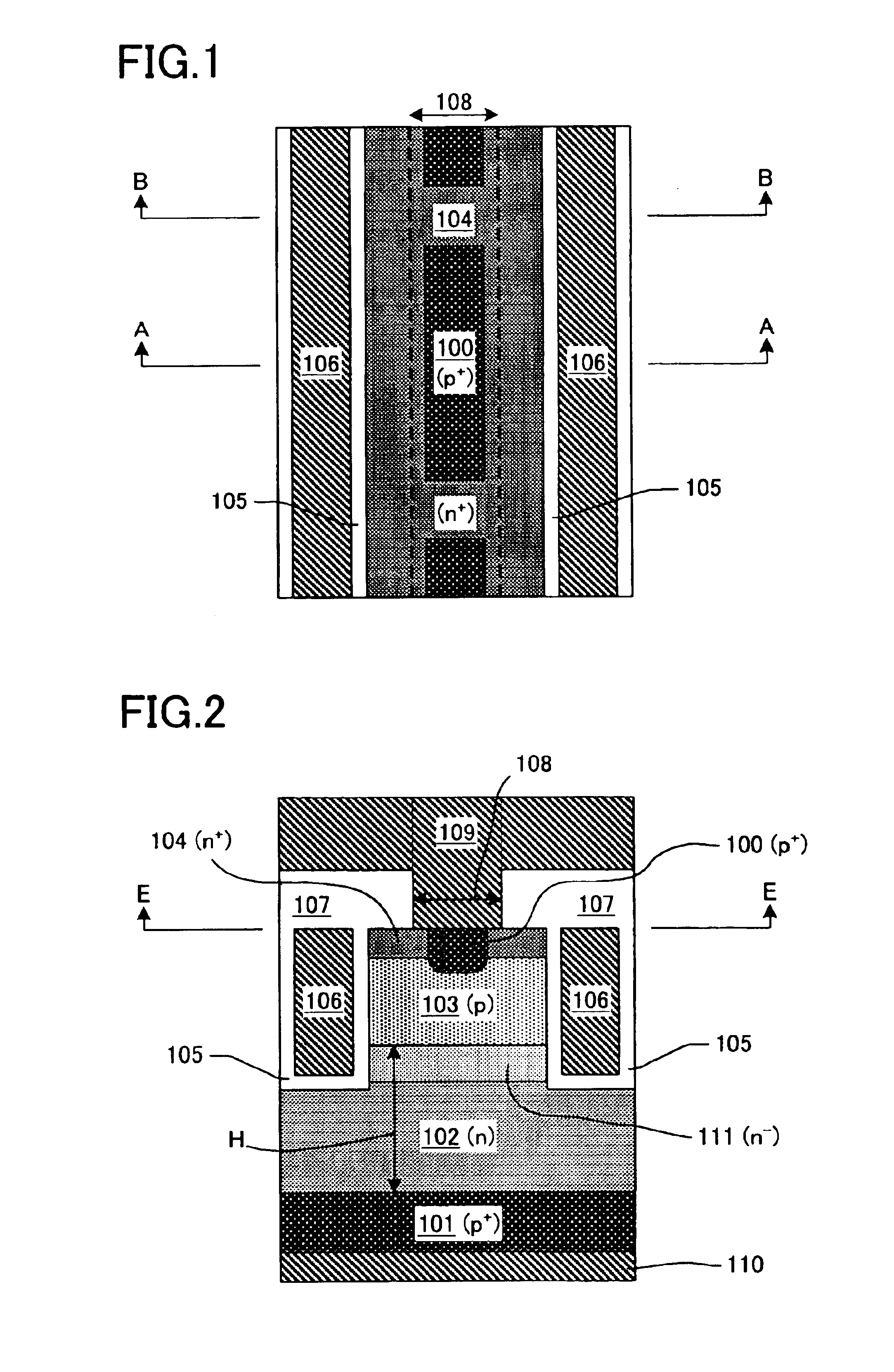
[0032]FIG. 1 through FIG. 3 show structure of a high withstand voltage field effect type semiconductor device directed to a first embodiment. FIG. 2 shows a sectional view of a portion A—A in FIG. 1. FIG. 3 shows a sectional view of a portion B—B in FIG. 1. FIG. 1 shows a sectional view of a portion E—E (this level is termed as “surface” in this specification) in FIG. 2 and in FIG. 3. This high withstand voltage field effect type semiconductor device is so-called an insulated gate-type bipolar transistor (IGBT) and has trench-structured gate electrodes 106. Roughly speaking, this high withstand voltage field effect type semiconductor device is structured such that N+ emitter regions 100, 104 and gate electrodes 106 are arranged on a surface of a semiconductor substrate (upper side in FIG. 2 and in FIG. 3) and a P+ collector region 101 and the like are arranged on other face of the substrate (bottom side in FIG. 2 and in FIG. 3).

[0033]That is, P+ emitter regions 100...

second embodiment

[Second Embodiment]

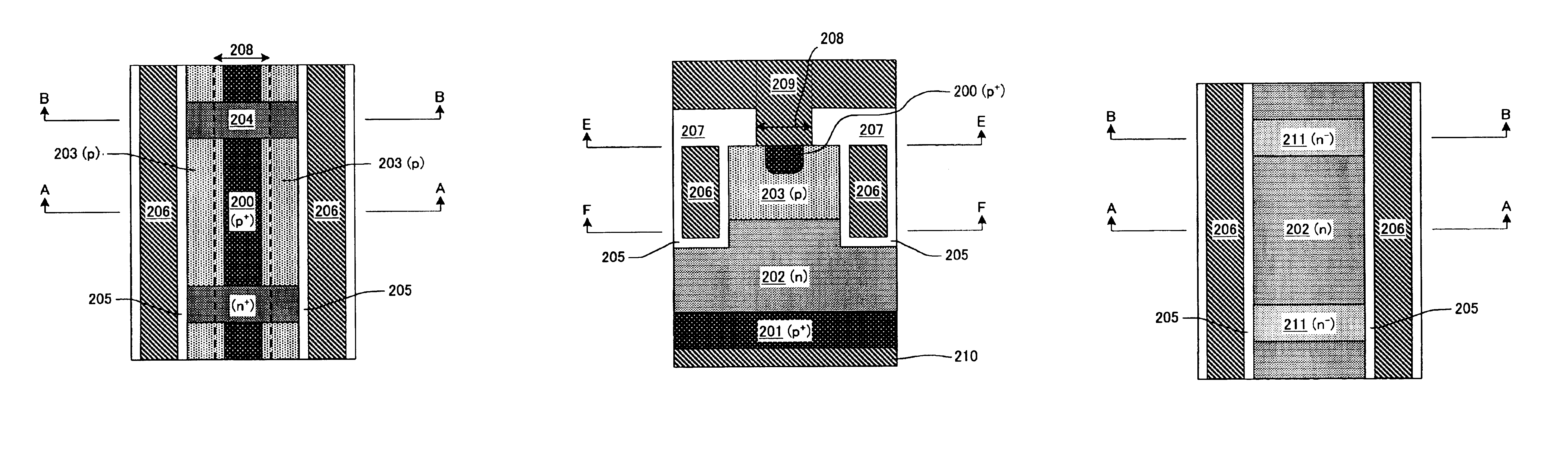
[0049]FIG. 10 through FIG. 12 show structure of a high withstand voltage field effect type semiconductor device directed to a second embodiment. FIG. 11 shows a sectional view of a portion A—A in FIG. 10 and in FIG. 12. FIG. 10 shows a sectional view of a portion E—E in FIG. 11. FIG. 12 shows a sectional view of a portion F—F in FIG. 11. Furthermore, the sectional view of the portion B—B in FIG. 10 and in FIG. 12 is substantially same as FIG. 3 for the first embodiment of which numberings are changed from “1**” to “2**”. Hereinafter, numberings should be interpreted like that when FIG. 3 is referred in this embodiment. The high withstand voltage field effect type semiconductor device of this embodiment is common to the first embodiment in terms of being trench-gate type. Furthermore, except for structure of emitter portion and N− field dispersion region, other structure of it is same as the first embodiment. Furthermore, P+ emitter regions 200 in its emitter porti...

third embodiment

[Third Embodiment]

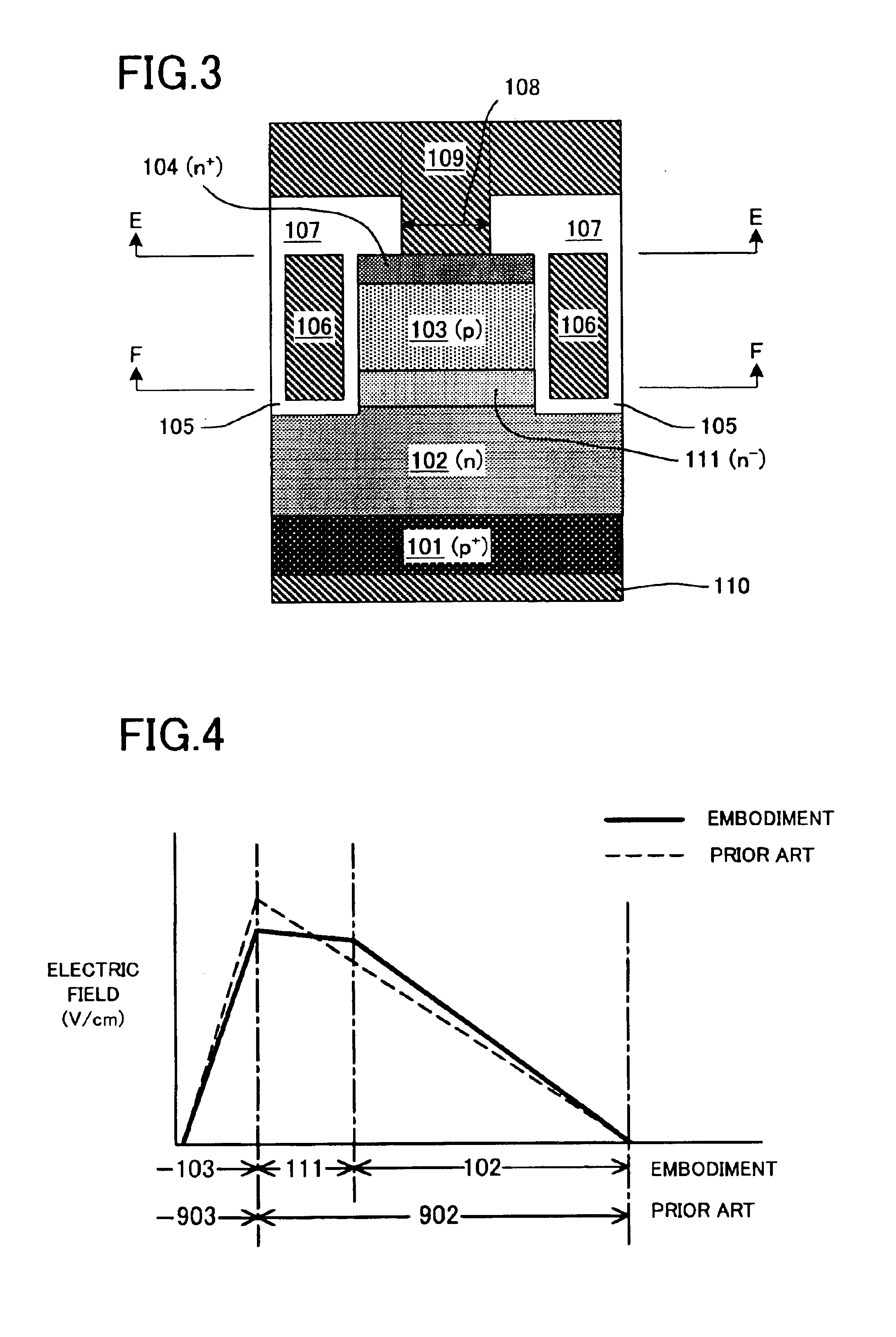
[0055]FIG. 13 and FIG. 14 show structure of a high withstand voltage field effect type semiconductor device directed to a third embodiment. The sectional view of the portion E—E in FIG. 13 and in FIG. 14 is substantially same as FIG. 10 for the second embodiment of which numberings are changed from “2**” to “3**”. Hereinafter, numberings should be interpreted like that when FIG. 10 is referred in this embodiment. FIG. 13 shows a sectional view of a portion A—A in FIG. 10. FIG. 14 shows a sectional view of a portion B—B in FIG. 10. The high withstand voltage field effect type semiconductor device of this embodiment is common to the first and second embodiments in terms of being trench-gate type. Furthermore, except for structure of an N− field dispersion region 311, other structure of it is same as the second embodiment.

[0056]There will be described an N− field dispersion region 311 of the high withstand voltage field effect type semiconductor device of this embodim...


PUM


Abstract

It is intended to provide a high withstand voltage field effect type semiconductor device that relaxes electric fields in a semiconductor substrate without thickening thickness of a drift region and achieves withstand-ability against high voltage without sacrificing ON-voltage, switch-OFF characteristics, and miniaturization. A field effective type semiconductor device comprises emitter regions 100, 104 and gate electrodes 106 and the like on a surface (upper surface in FIG. 2), a collector region 101 and the like on the other surface (lower surface in FIG. 2), wherein N− field dispersion regions 111 of low impurity concentration are arranged between P body regions 103 facing to gate electrodes 106 and an N drift region 102 below P body regions 103. Thereby, electric field between collector and emitter is relaxed and high withstand voltage field effect type semiconductor device is realized. Another field dispersion region can be arranged between the N drift region 102 and P+ collector region 101 below the N drift region 102.

Description

BACKGROUND OF THE INVENTION[0001]1. Field of the Invention[0002]The present invention relates to a field effect type semiconductor device provided with a body region that receives field effect of a gate electrode and a drift region arranged below the body region. More particularly, it relates to a high withstand voltage field effect type semiconductor device that achieves to enhance withstand-ability against higher voltage without sacrificing ON-voltage.[0003]2. Description of Related Art[0004]There have conventionally been used field effect type semiconductor devices for power devices (for example, JP Laid-open Patent Publication 09-283754, and the like). This type of field effect type semiconductor device has structure such as shown in FIG. 20, in general. A sectional view of a portion E—E is substantially same as FIG. 1 of which numberings are changed from “1**” to “9**”. Hereinafter, numbering should be interpreted like that when FIG. 1 is referred in the description of related ...

Claims


Application Information

Patent Timeline
IPC IPC(8): H01L21/331H01L29/06H01L29/08H01L21/02H01L29/739H01L29/02H01L29/66H01L29/78
CPCH01L29/0696H01L29/0834H01L29/66348H01L29/7813
Inventor NISHIWAKI, KATSUHIKOKUSHIDA, TOMOYOSHIKAWAJI, SACHIKO
Owner TOYOTA JIDOSHA KK
Why Eureka
Try Eureka