Machining method of metal packaging shell of large-scale and large-power integrated circuit
An integrated circuit and metal packaging technology, which is applied in the manufacture of circuits, electrical components, semiconductors/solid-state devices, etc., can solve the problem of not being able to reach industrial production, not fully satisfying the processing of large-scale high-power integrated circuit shells, and not fully satisfying the product environment Adaptability and other issues
- Summary
- Abstract
- Description
- Claims
- Application Information
AI Technical Summary
Problems solved by technology
Method used
Image
Examples
Embodiment 1
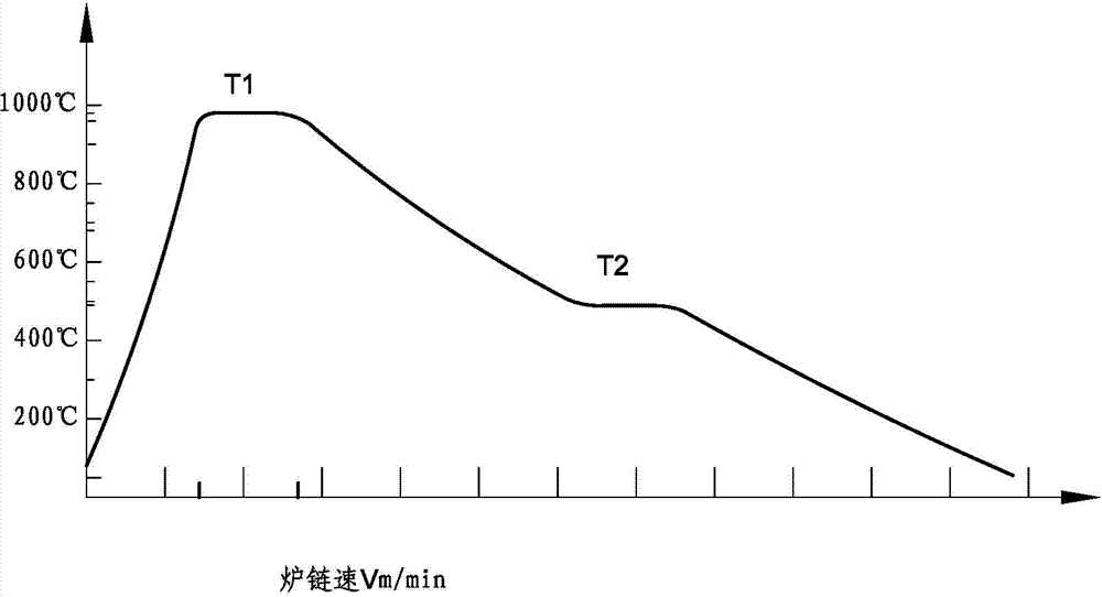
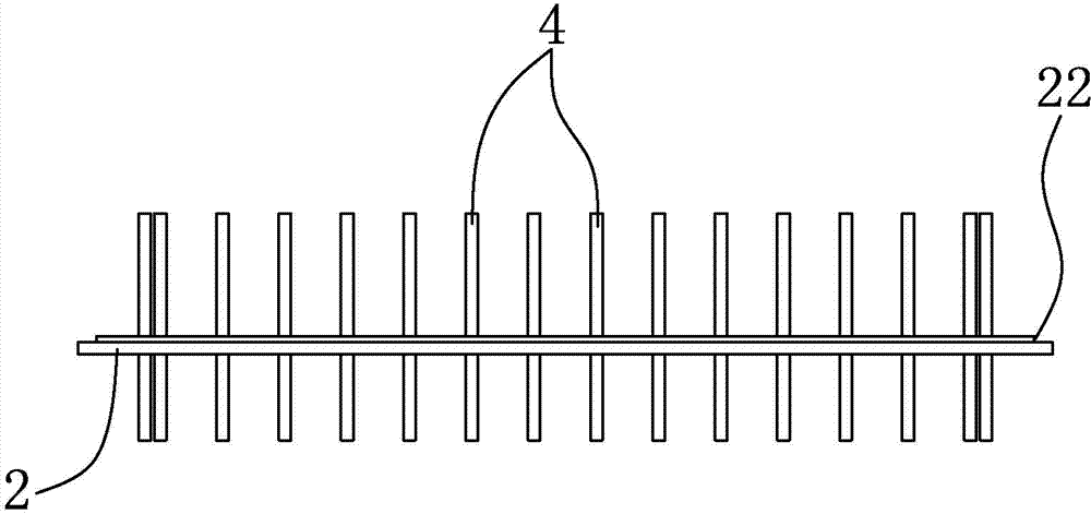
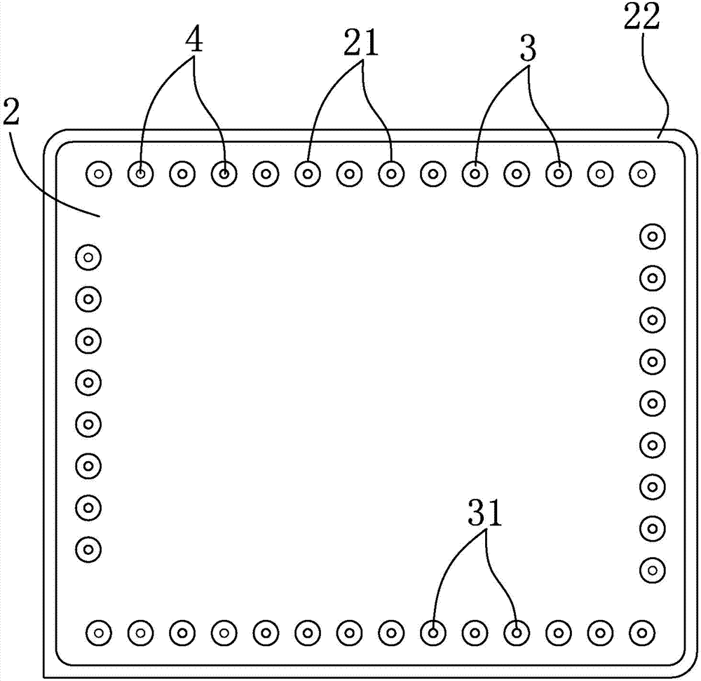
[0046] For the processing method of large-scale and high-power integrated circuit metal packaging shell, see figure 2 — Figure 5 , the shell includes a base and an outer cover 1, the base is composed of a base plate 2, forty-five glass blanks 3, and forty-five lead pins 4, and the base plate 2 is provided with forty-five pins for placing lead pins 4 and glass blanks. 3 through the first through hole 21, the lead pin 4 is placed in the first through hole 21 on the bottom plate 2 through the glass gob 3;
[0047] The processing method of the base includes the following process steps:
[0048] (1) Use the processing center LMC-1000 to process the Kovar alloy sheet material 4J29 into a rectangular bottom plate 2 with forty-five first through holes 21 for placing the lead pins 4 and the glass blank 3. The periphery of the bottom plate 2 is provided with Place the step 22 of the outer cover 1, after the machining is completed, sandblast the surface of the bottom plate 2, and then ...
Embodiment 2
[0057] For the processing method of large-scale and high-power integrated circuit metal packaging shell, see figure 2 — Figure 5 , the shell includes a base and an outer cover 1, the base is composed of a base plate 2, forty-five glass blanks 3, and forty-five lead pins 4, and the base plate 2 is provided with forty-five pins for placing lead pins 4 and glass blanks. 3 through the first through hole 21, the lead pin 4 is placed in the first through hole 21 on the bottom plate 2 through the glass gob 3;
[0058] The processing method of the base includes the following process steps:
[0059] (1) Use the processing center LMC-1000 to process the Kovar alloy sheet material 4J29 into a rectangular bottom plate 2 with forty-five first through holes 21 for placing the lead pins 4 and the glass blank 3. The periphery of the bottom plate 2 is provided with Place the step 22 of the outer cover 1, after the machining is completed, sandblast the surface of the bottom plate 2, and the...
PUM
| Property | Measurement | Unit |
|---|---|---|
| Insulation resistance | aaaaa | aaaaa |
Abstract
Description
Claims
Application Information


