

Electro-optical device and electronic apparatus
a technology of optical devices and electronic devices, applied in static indicating devices, non-linear optics, instruments, etc., can solve problems such as inability to resolve and achieve excellent appearance and reduce display irregularities in series
- Summary
- Abstract
- Description
- Claims
- Application Information
AI Technical Summary
Benefits of technology
Problems solved by technology
Method used
Image

Examples
first embodiment
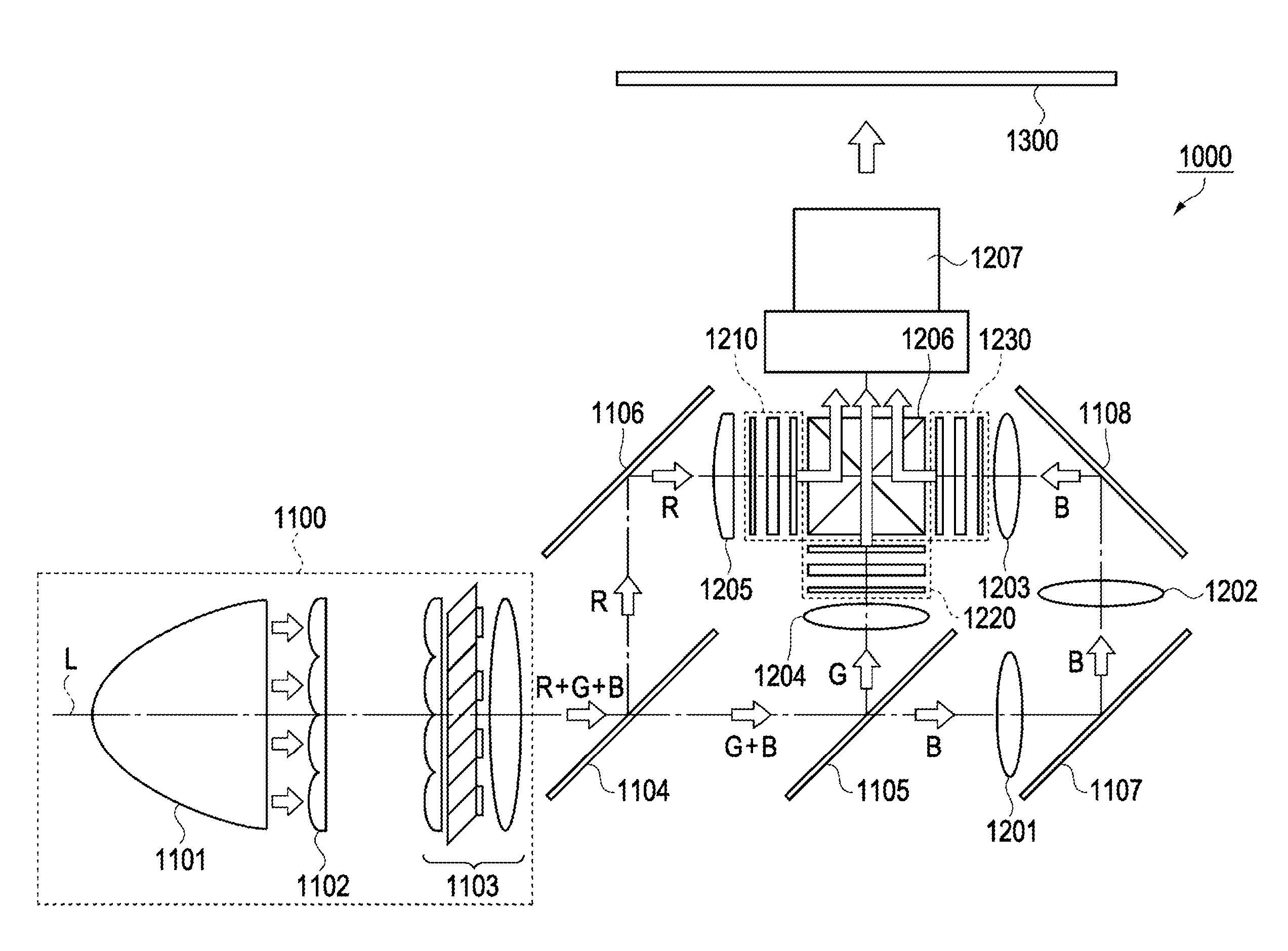
[0034]The present embodiment is described with an active matrix type liquid crystal device which is provided with a thin film transistor (TFT) as a pixel switching element as an example of an electro-optical device. It is possible for this liquid crystal device to be appropriately used as, for example, an optical modulation element (liquid crystal light valve) of a projector type display device (liquid crystal projector) which will be described later.
[0035]Liquid Crystal Device
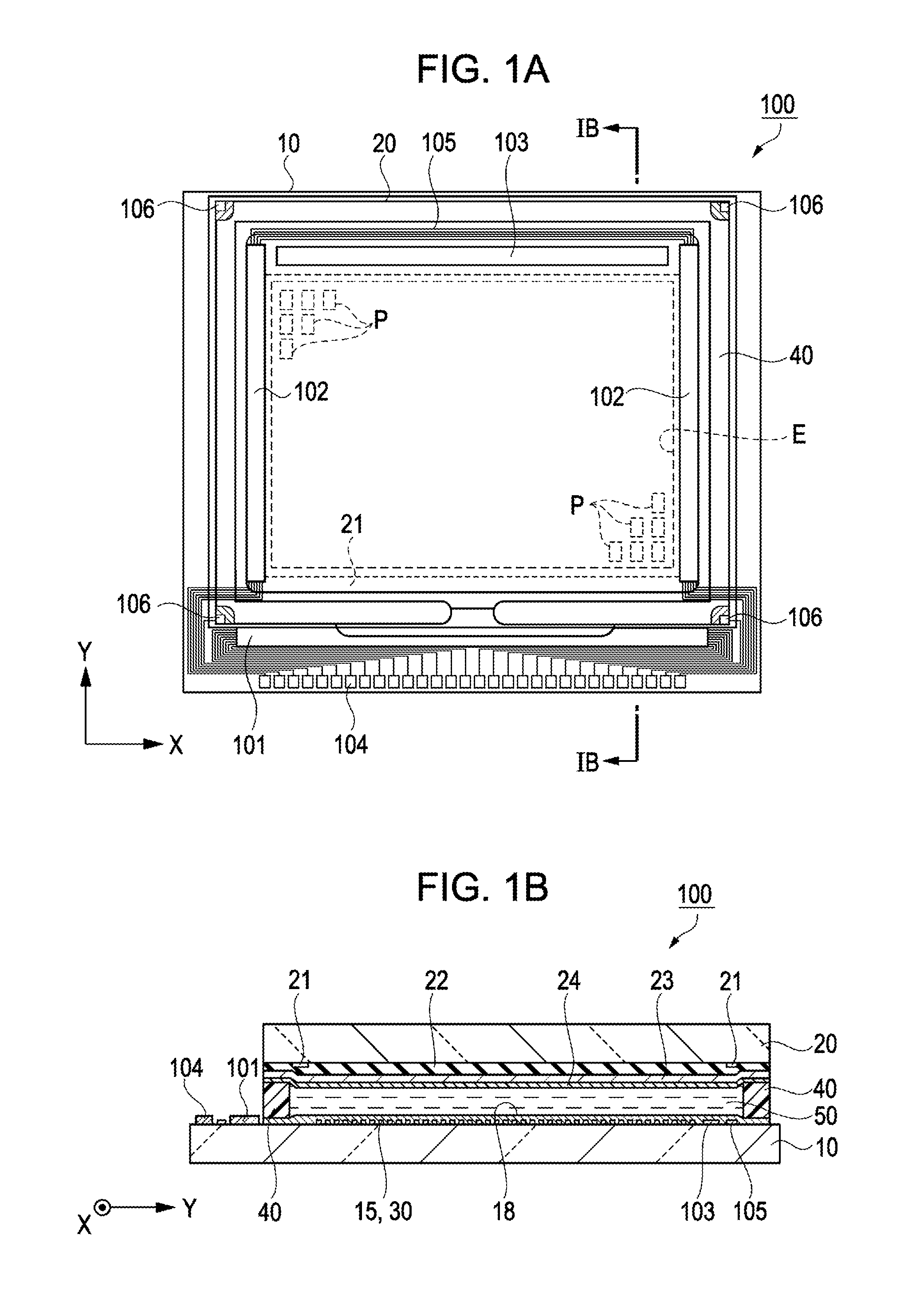
[0036]First, a schematic structure of a liquid crystal device as the electro-optical device of the present embodiment will be described with reference to FIGS. 1A and 1B. FIG. 1A is a schematic planar view illustrating a configuration of a liquid crystal device and FIG. 1B is a schematic cross-sectional view along a line IB-IB of the liquid crystal device illustrated in FIG. 1A.
[0037]As illustrated in FIGS. 1A and 1B, a liquid crystal device 100 as the electro-optical device of the present embodiment has an el...
second embodiment
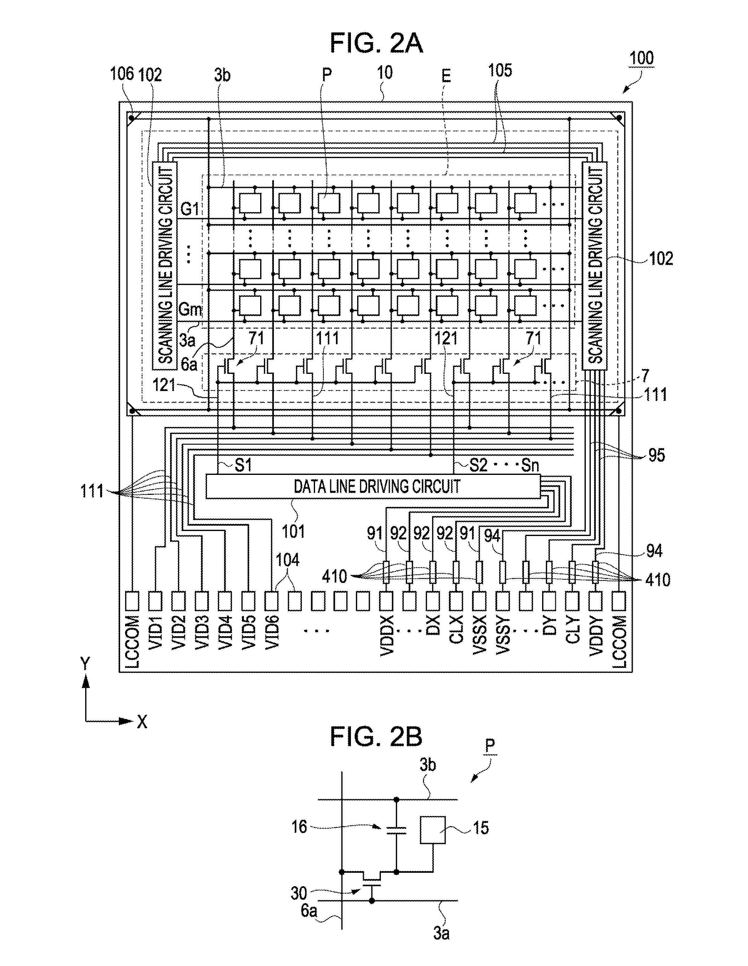
[0079]Next, a liquid crystal device of a second embodiment will be described with reference to FIG. 5. FIG. 5 is a circuit diagram illustrating a main circuit configuration of the liquid crystal device according to the second embodiment. The liquid crystal device according to the second embodiment differs in terms of the method of driving the plurality of data lines 6a with regard to the liquid crystal device 100 of the first embodiment. Accordingly, the same reference numerals are attached to the same configurations as the liquid crystal device 100 and the detailed description is omitted.
[0080]As shown in FIG. 5, a liquid crystal device 200 of the present embodiment has a plurality of the pixels P which are partitioned by a plurality of the scanning lines 3a and a plurality of the data lines 6a and are arranged in a matrix formation in the pixel region E on the element substrate 10 side. In addition, a semiconductor integrated circuit (IC) 201 as a driving circuit which drives the ...
third embodiment
[0091]Next, a liquid crystal device of the third embodiment will be described with reference to FIG. 6. FIG. 6 is a circuit diagram illustrating a main circuit configuration of the liquid crystal device according to the third embodiment. The liquid crystal device of the third embodiment is an example where the hybrid driving method of the second embodiment is applied to 4k2k, so-called super Hi-Vision, which has four times the number of pixel of Hi-Vision (number of pixels; 1920×1080). Here, in FIG. 6, the circuit configuration of the main portions is shown and the circuit configuration across all of the pixels P is not shown. The same configurations as the liquid crystal device 200 of the second embodiment are given the same reference numeral and a detailed description is omitted.
[0092]As shown in FIG. 6, a liquid crystal device 300 has a plurality (4096×2160) of the pixels P which are partitioned by a plurality of scanning lines and a plurality of data lines and are arranged in a ...
PUM
 Abstract
Description
Claims
Application Information