
Semiconductor device

a technology of semiconductor devices and semiconductor devices, applied in pulse manipulation, pulse technique, instruments, etc., can solve the problems of performance and reliability degradation of semiconductor devices,

Active Publication Date: 2017-02-02
SK HYNIX INC
View PDF3 Cites 3 Cited by
  • Summary
  • Abstract
  • Description
  • Claims
  • Application Information

AI Technical Summary

Benefits of technology

This patent aims to protect semiconductor elements from stress caused by negative bias temperature instability (NBTI) during precharge and stress sections. The technical effects of the patent text are to minimize the impact of NBTI on the performance and reliability of semiconductor devices.

Problems solved by technology

Continuous operation of semiconductor devices may result in performance and reliability degradation due to stress.
Particularly, PMOS transistors comprised in a semiconductor device may deteriorate due to a phenomenon known as Negative Bias Temperature Instability (NBTI), and therefore, performance of the semiconductor device may also deteriorate.
As a result, one or more timing relations set inside a semiconductor device may change, and consequently, performance and reliability of the semiconductor device may deteriorate.
Performance and reliability of the semiconductor device remains substantially unaffected over an extended period of time of operation.

Method used


Image

  • Semiconductor device
  • Semiconductor device
  • Semiconductor device

Examples


Embodiment Construction

[0035]Various embodiments of the present invention are described below with reference to the accompanying drawings. These embodiments are provided so that this disclosure is thorough and complete and are not intended to limit the scope of the invention.

[0036]The terminology used herein is for the purpose of describing particular embodiments of the invention only and is not intended to be limiting of the inventive concept. As used herein, the singular forms “a”, “an” and “the” are intended to include the plural forms as well, unless the context clearly indicates otherwise. It will be further understood that the terms “comprises” and / or “comprising,” when used in this specification, indicate the presence of stated features, but do not preclude the presence or addition of one or more other features. As used herein, the term “and / or” indicates any and all combinations of one or more of the associated listed items. It is also noted that in this specification, “connected / coupled” refers t...


PUM


Abstract

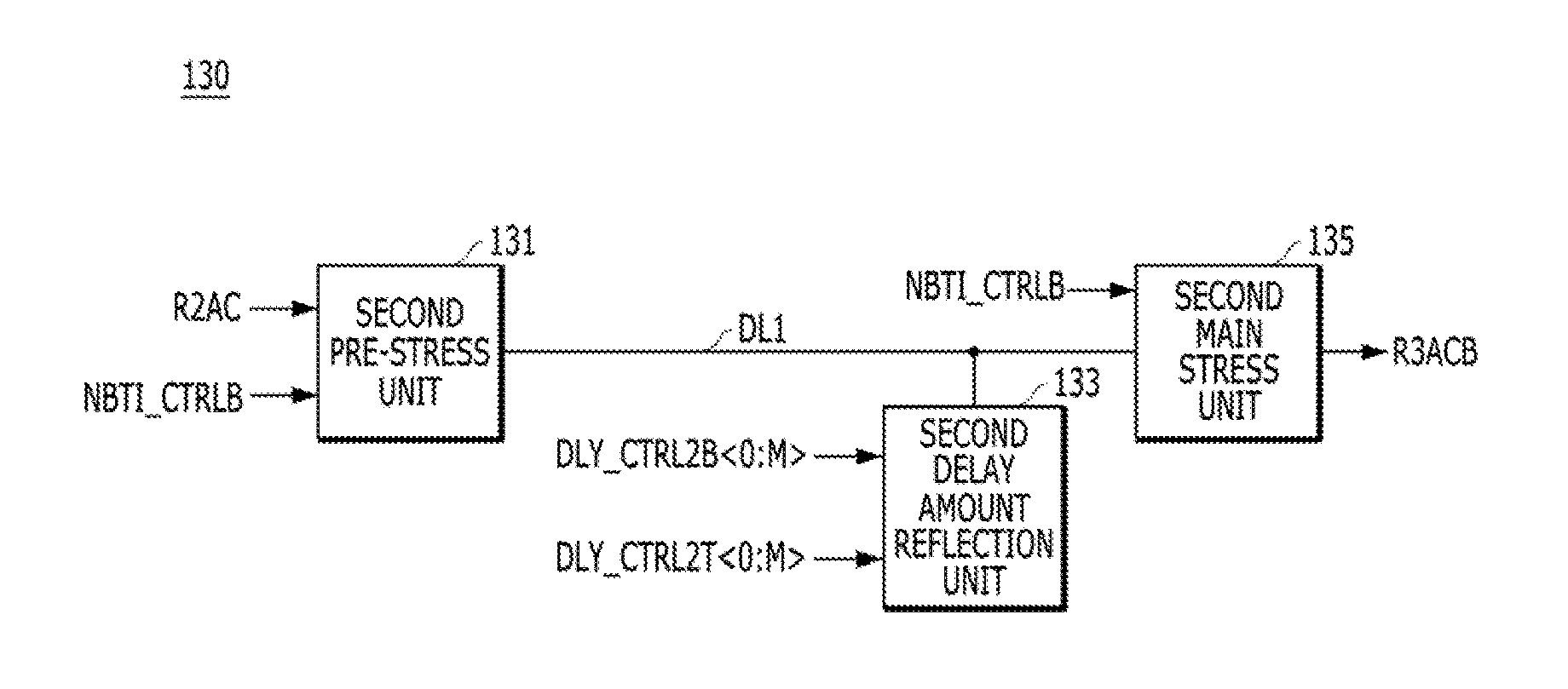
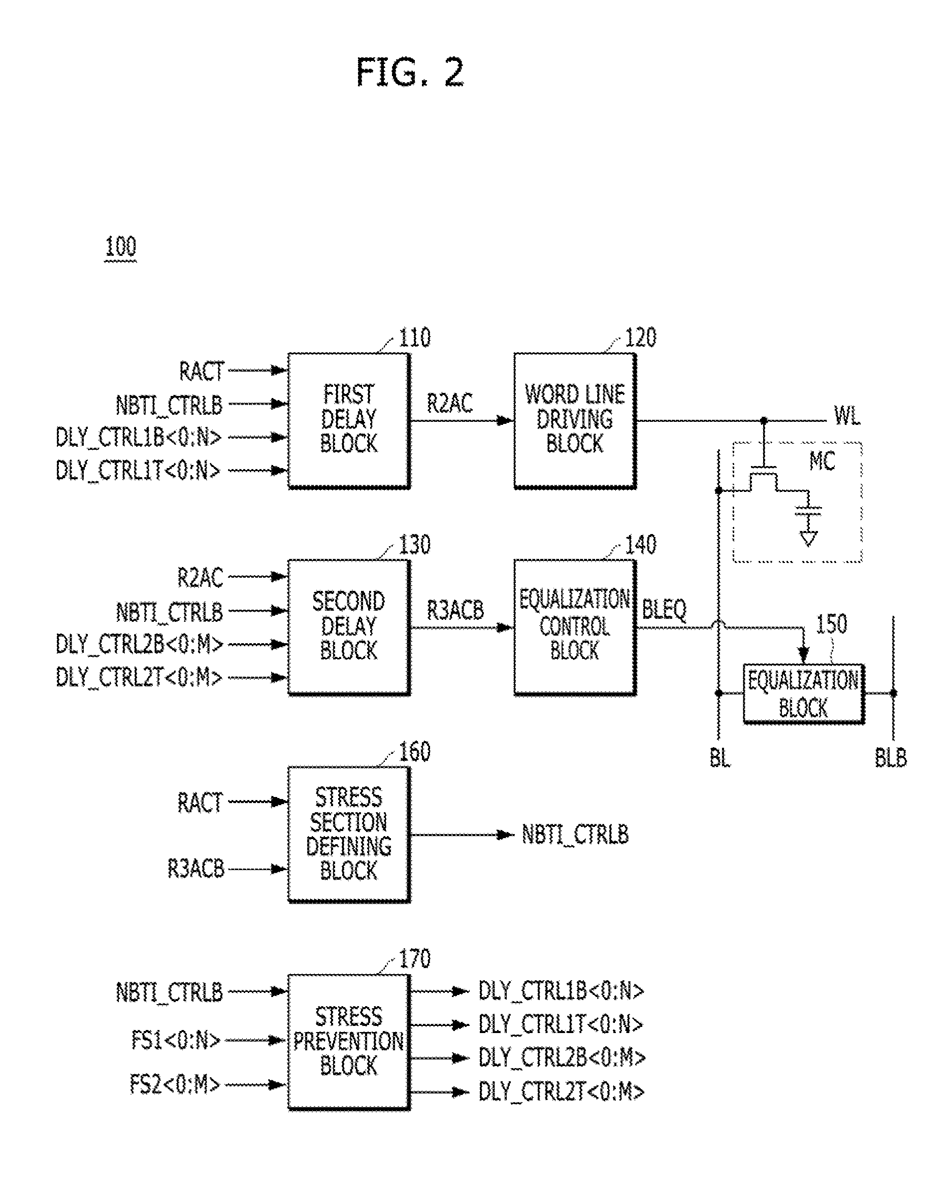
A semiconductor device includes a first pre-stress block suitable for generating a first load signal, which corresponds to an active signal during an active mode and / or to a high voltage level during a precharge mode, in response to a stress section signal; a first delay amount reflection block suitable for reflecting a first delay amount in the first load signal in response to one or more first delay amount control signals; and a first main stress block suitable for generating a word line driving control signal, which corresponds to the active signal during the active mode and the high voltage level during the precharge mode, in response to the stress section signal and the first load signal.

Description

CROSS-REFERENCE TO RELATED APPLICATIONS[0001]The present application claims priority from Korean Patent Application No. 10-2015-0106393, filed on Jul. 28, 2015, which is incorporated herein by reference in its entirety.BACKGROUND[0002]1. Field[0003]Various embodiments of the present invention relate to a semiconductor design technology, and more particularly to a semiconductor device.[0004]2. Description of the Related Art[0005]Continuous operation of semiconductor devices may result in performance and reliability degradation due to stress. Particularly, PMOS transistors comprised in a semiconductor device may deteriorate due to a phenomenon known as Negative Bias Temperature Instability (NBTI), and therefore, performance of the semiconductor device may also deteriorate.[0006]According to the NBTI phenomenon, the threshold voltage of a PMOS transistor may increase due to stress and the PMOS transistor may be disturbed to form channels while the PMOS transistor is continuously turned...

Claims


Application Information

Patent Timeline
IPC IPC(8): H03K5/14H03K3/037G11C11/4076G11C11/4093G11C11/4094
CPCH03K5/14G11C11/4093H03K2005/00019G11C11/4076H03K3/037G11C11/4094H03K5/06H03K5/131H03K19/00384G11C7/04G11C7/12G11C8/08G11C11/4085
Inventor CHI, SUNG-SOOHEO, YOUNG-SIK
Owner SK HYNIX INC
Learn More