Placement machine and method for equipping a substrate with unhoused chips

a technology of placement machine and substrate, which is applied in the direction of electrical apparatus, printed circuit assembling, and semiconductor devices, etc., can solve the problems of difficult to observe a high placement accuracy, large or long substrates, and insufficient positioning accuracy of substrates, so as to achieve accurate definition and improve the accuracy of substrate positioning determination in the coordinate system of the placement machine.

Active Publication Date: 2017-02-02
ASMPT GMBH & CO KG
View PDF5 Cites 2 Cited by
  • Summary
  • Abstract
  • Description
  • Claims
  • Application Information

AI Technical Summary

Benefits of technology

[0076]In a simple exemplary embodiment the two optical structures can be simply two holes, which are applied to or formed on the substrate at an edge, in particular in opposing positions. The use of simple holes as optical structures has the advantage that these holes can also be used for a mechanical handling of the substrate, for example by means of centering pins.
[0077]It should also be noted that the substrate to be equipped can of course also have more than two optically identifiable structures. The accuracy of the positioning determination of the substrate in the coordinate system of the placement machine can thus be further improved.
[0078]The two optical structures of the substrate can also be used, after a, for example, pneumatic fixing of the substrate to the one-piece support element, to model the substrate as a rigid fixed body (that is to say without warping), such that each possible placement position on the substrate with respect to the two optical structures is accurately defined.

Problems solved by technology

Here, substrates can also be so large or long that they must be moved along a transport direction during the course of a placement process taking a very long time.
In this regard, it is clear that large or long substrates make it additionally difficult to observe a high placement accuracy.

Method used


Image

  • Placement machine and method for equipping a substrate with unhoused chips
  • Placement machine and method for equipping a substrate with unhoused chips
  • Placement machine and method for equipping a substrate with unhoused chips

Examples


Embodiment Construction

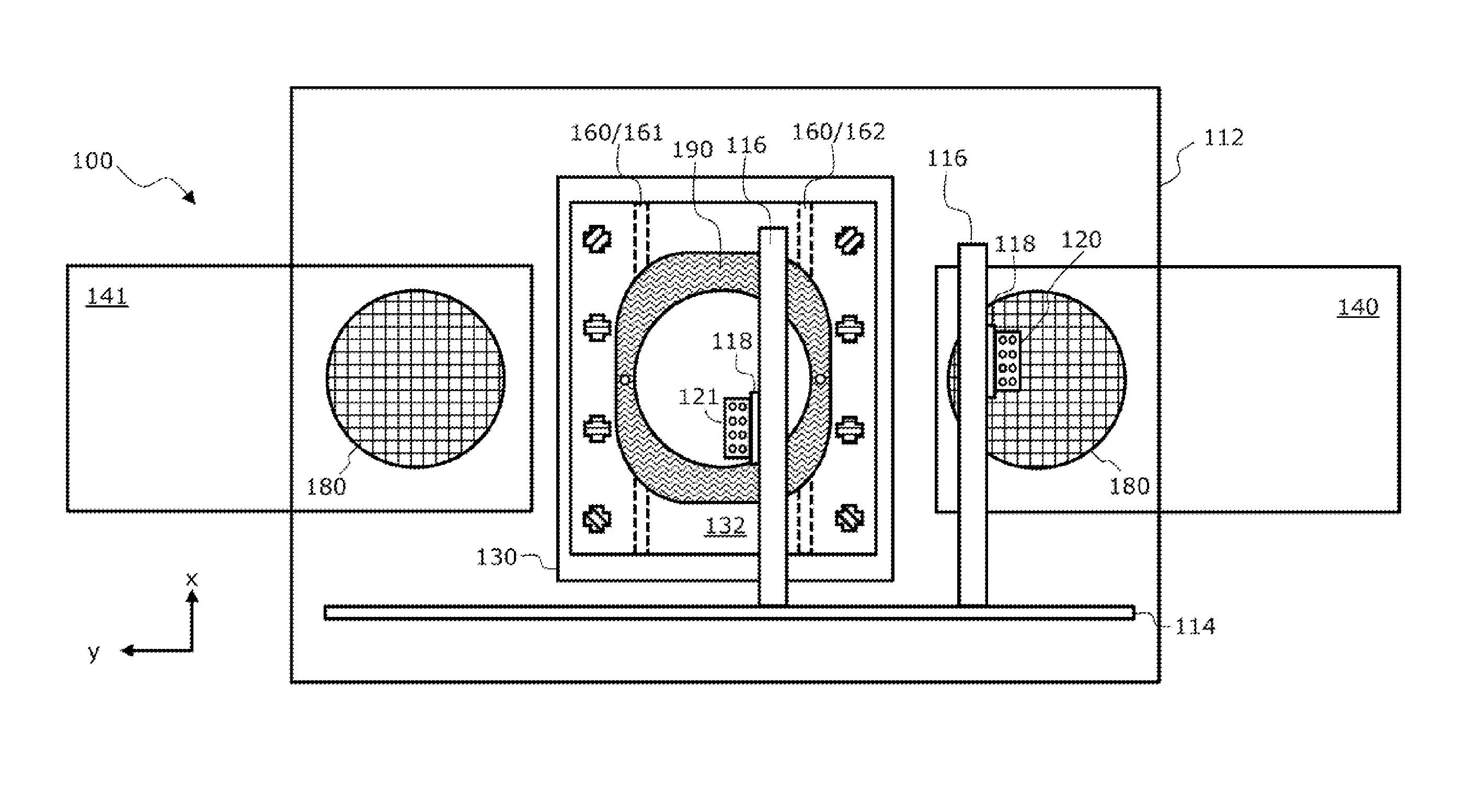
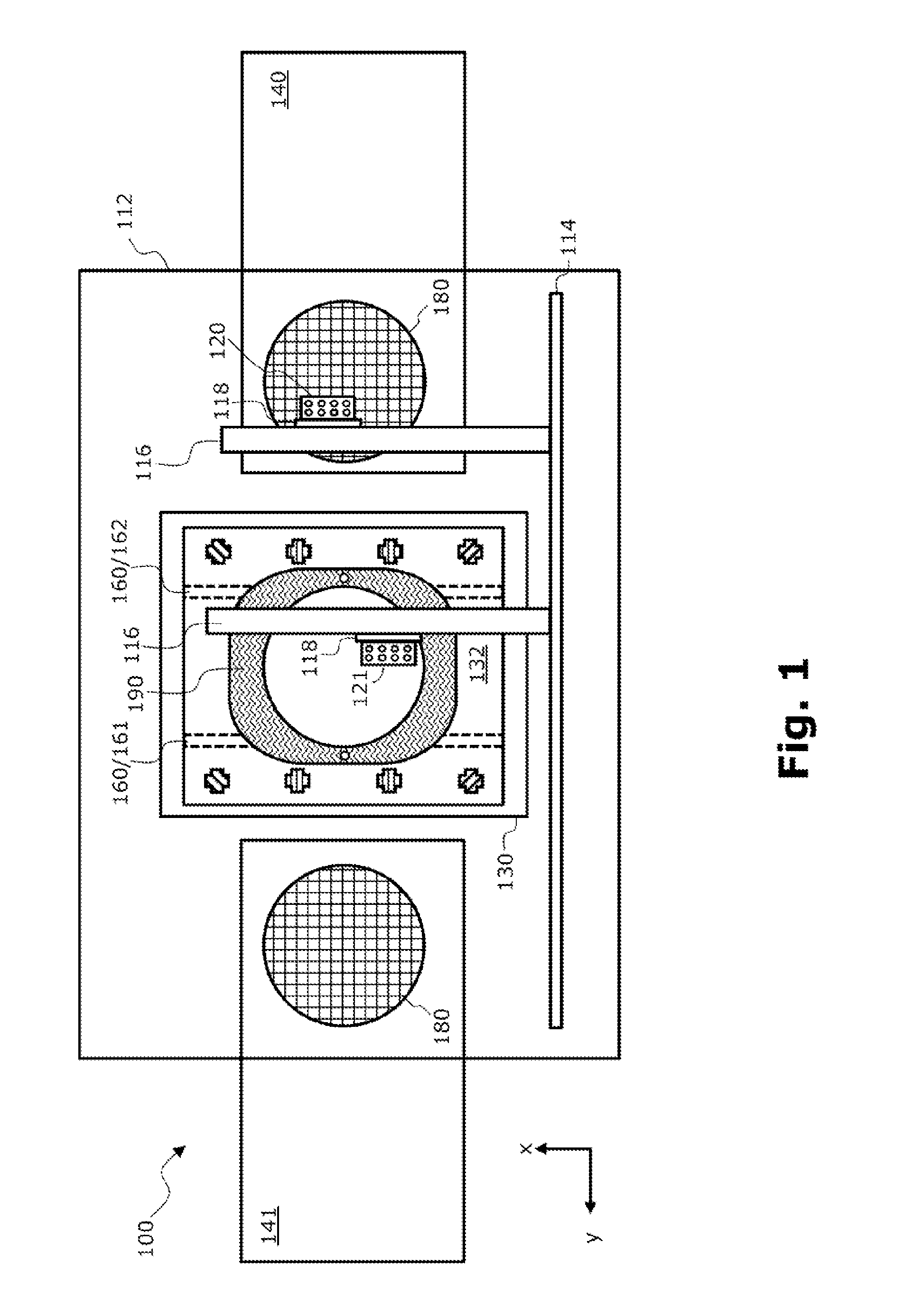
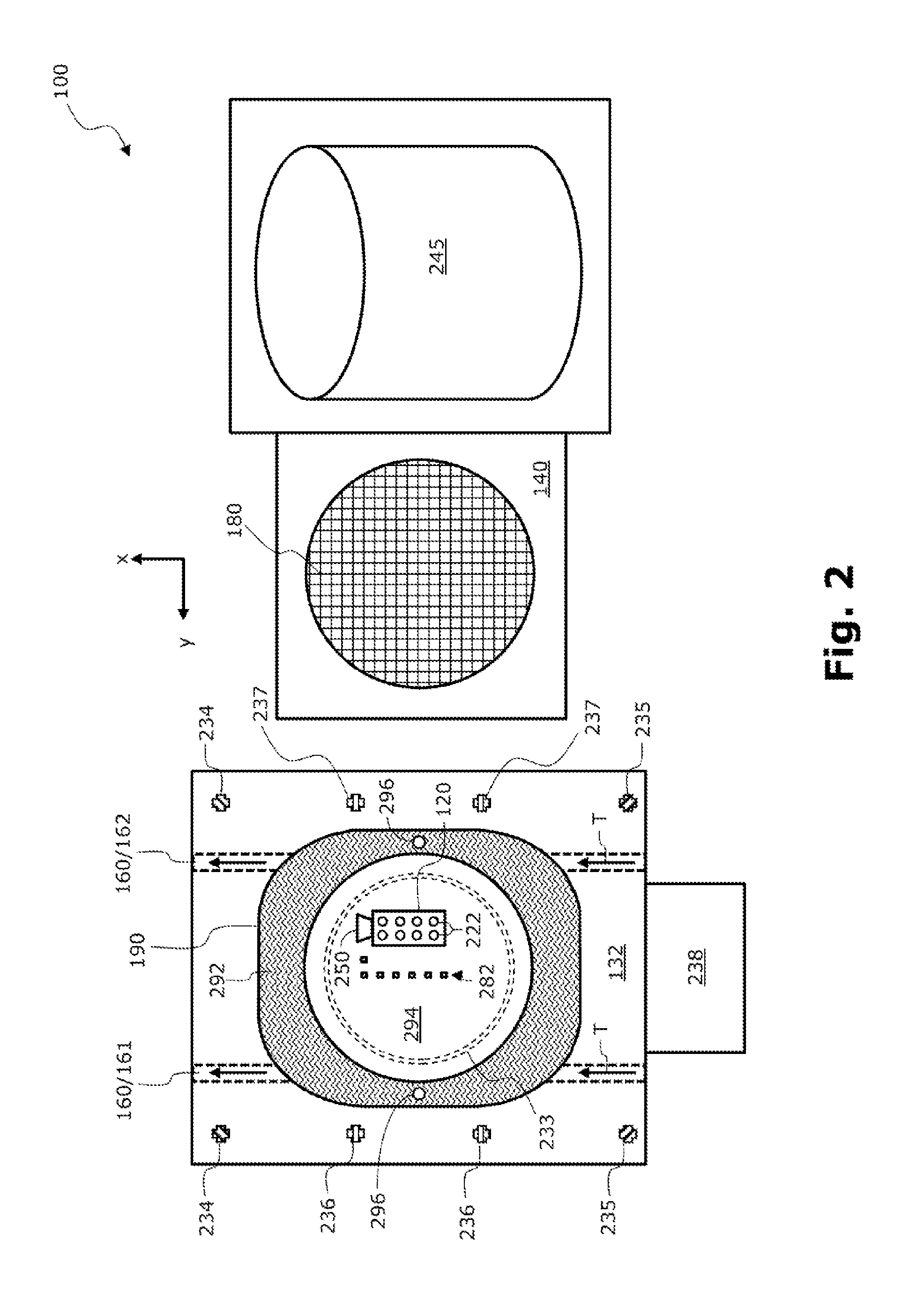
[0097]It should be noted that, in the following detailed description, features or components of different embodiments which are identical or at least functionally identical to the corresponding features or components of another embodiment are provided with the same reference signs or with a reference sign which differs from the reference sign of the identical or at least functionally identical features or components merely by the first number. In order to avoid unnecessary repetitions, features or components already explained on the basis of a previously described embodiment will not be described in greater detail at a subsequent point.

[0098]It should also be noted that the embodiments described hereinafter constitute merely a limited selection of possible variants of the invention. In particular, it is possible to suitably combine the features of individual embodiments with one another such that, with the variants presented explicitly here, a large number of different embodiments a...


PUM

PropertyMeasurementUnit
temperatureaaaaaaaaaa
pressureaaaaaaaaaa

Abstract

What is described is a placement machine (100, 300, 500) for equipping a substrate (190) with unhoused chips (282). The placement machine (100, 300, 500) has (a) a chassis (112); (b) a feed device (140) for providing a wafer (180) which has a multiplicity of chips (282), wherein the feed device (140) is mounted on the chassis (112); (c) a lifting device (513), which is mounted on the chassis (112); (d) a substrate-receiving device (130) for receiving the substrate (190) to be equipped, wherein the substrate-receiving device (130) is mounted on the lifting device (513) and can be moved relative to the chassis (112) along a z-direction by means of the lifting device (513); and (e) a placement head (120) for picking up chips (282) from the provided wafer (180) and for placing the picked-up chips (282) at predefined placement positions on the received substrate (190). The substrate-receiving device (130) has (d1) a one-piece support element (132, 332, 532), which constitutes at least an upper part of the substrate-receiving device (130), wherein the substrate (190) to be equipped can be laid on the one-piece support element (132, 332, 532); and (d2) a transport device (160) for transporting the substrate (190) on an upper side of the one-piece support element (132, 332, 532) along a transport direction (T). The transport device (160) is spatially integrated in the one-piece support element (132, 332, 532) on the upper side of the one-piece support element (132, 332, 532). A method for equipping a substrate (190) with unhoused chips (282) using a placement machine (100, 300, 500) of this type is also described.

Description

TECHNICAL FIELD[0001]The present invention relates in general to the technical field of production of electronic components. The present invention in particular relates to a placement machine and to a method for handling unhoused chips within the scope of manufacture of electronic components which each have at least one chip packaged in a housing and suitable electrical connection contacts by means of which the packaged chip can be electrically contacted.BACKGROUND OF THE INVENTION[0002]When manufacturing housed electronic components, unhoused (semiconductor) chips, or what are known as “bare dies”, are placed on a substrate. Within the scope of what is known as the “embedded Wafer Level Package” (eWLP) process, one or more chips per package are for this purpose placed with the active side down onto an adhesive film disposed on the substrate. A multiplicity of set-down chips are then potted using a compound made of plastic, which later constitutes the housing. The entire potted prod...

Claims


Application Information

Patent Timeline
Patent Type & Authority Applications(United States)
IPC IPC(8): H05K3/30
CPCH05K3/30H01L21/67121H01L21/67144Y10T29/4913H01L21/52H01L21/67712H01L21/67721H01L24/01H01L24/74
Inventor PRUEFER, MARTIN
Owner ASMPT GMBH & CO KG
Why Eureka
Try Eureka