Semiconductor device

a semiconductor chip and shielding technology, applied in the direction of stacked capacitors, fixed capacitor details, thin/thick film capacitors, etc., can solve the problems of increasing reducing and unable to obtain the expected operation of the lsi at high frequencies, so as to reduce the wiring distance from the semiconductor chip die-bonded face up to the support of the capacitor, the noise reduction effect of the capacitor can be increased, and the wiring distan

Active Publication Date: 2017-02-09
NODA SCREEN
View PDF2 Cites 8 Cited by
  • Summary
  • Abstract
  • Description
  • Claims
  • Application Information

AI Technical Summary

Benefits of technology

[0021]According to this configuration, in the configuration in which the semiconductor chip and the external connection portions are connected via wire bonding, the wiring distance from the semiconductor chip to the capacitor can be decreased.
[0022]According to the present invention, there is provided a semiconductor device in which the wiring distance from the semiconductor chip die-bonded face up to the support to the capacitor is decreased, whereby the noise reduction effect of the capacitor can be increased and the reliability of the semiconductor chip during high frequency operation can be increased.

Problems solved by technology

However, as the clock frequency of semiconductor chips (LSI) has increased in recent years, when the wiring distance from the LSI to a capacitor is large, the high frequency impedance due to the wiring is increased.
As a result, the noise reduction effect of the capacitor decreases, which may cause the problem that an expected operation of the LSI cannot be obtained at high frequencies.

Method used


Image

  • Semiconductor device
  • Semiconductor device
  • Semiconductor device

Examples


first embodiment

[0034]A first embodiment of the present invention will be described with reference to FIG. 1 to FIG. 5.

1. Configuration of the Semiconductor Device of the First Embodiment

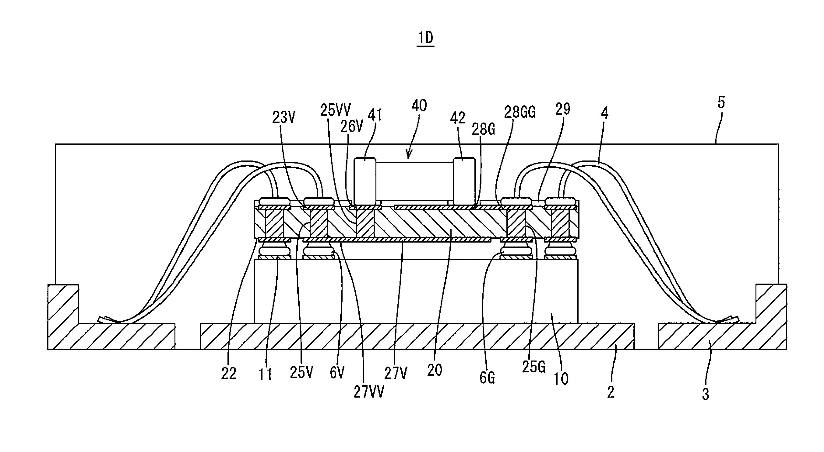
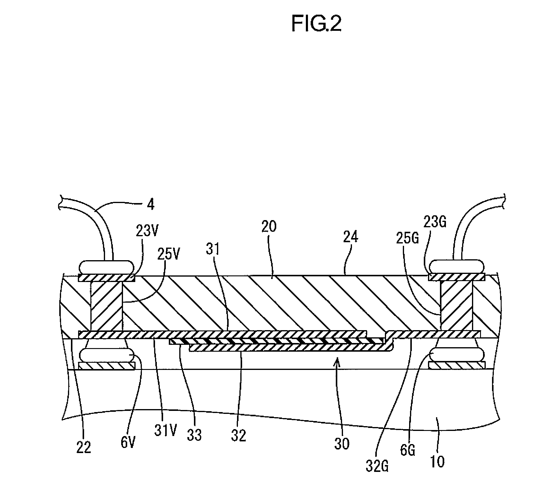
[0035]As illustrated in FIG. 1, a semiconductor device 1 according to the first embodiment is a Quad Flat No-Lead Package (QFN) semiconductor device. The semiconductor device 1, as illustrated in FIG. 1, is provided with a support 2 and an LSI chip (an example of “semiconductor chip”) 10 die-bonding mounted face up on the support 2. The semiconductor device 1 is also provided with a plurality of external connection portions 3 electrically connecting the LSI chip 10 to the outside; an intermediate substrate 20 provided on the side of the LSI chip 10 opposite from the support 2 and connecting the LSI chip 10 to the plurality of external connection portions 3; and a plurality of connection bumps 6 connecting the LSI chip 10 and the intermediate substrate 20.

[0036]The LSI chip 10 includes a plurality of electrode pads ...

second embodiment

5. Configuration of the Semiconductor Device according to the Second Embodiment

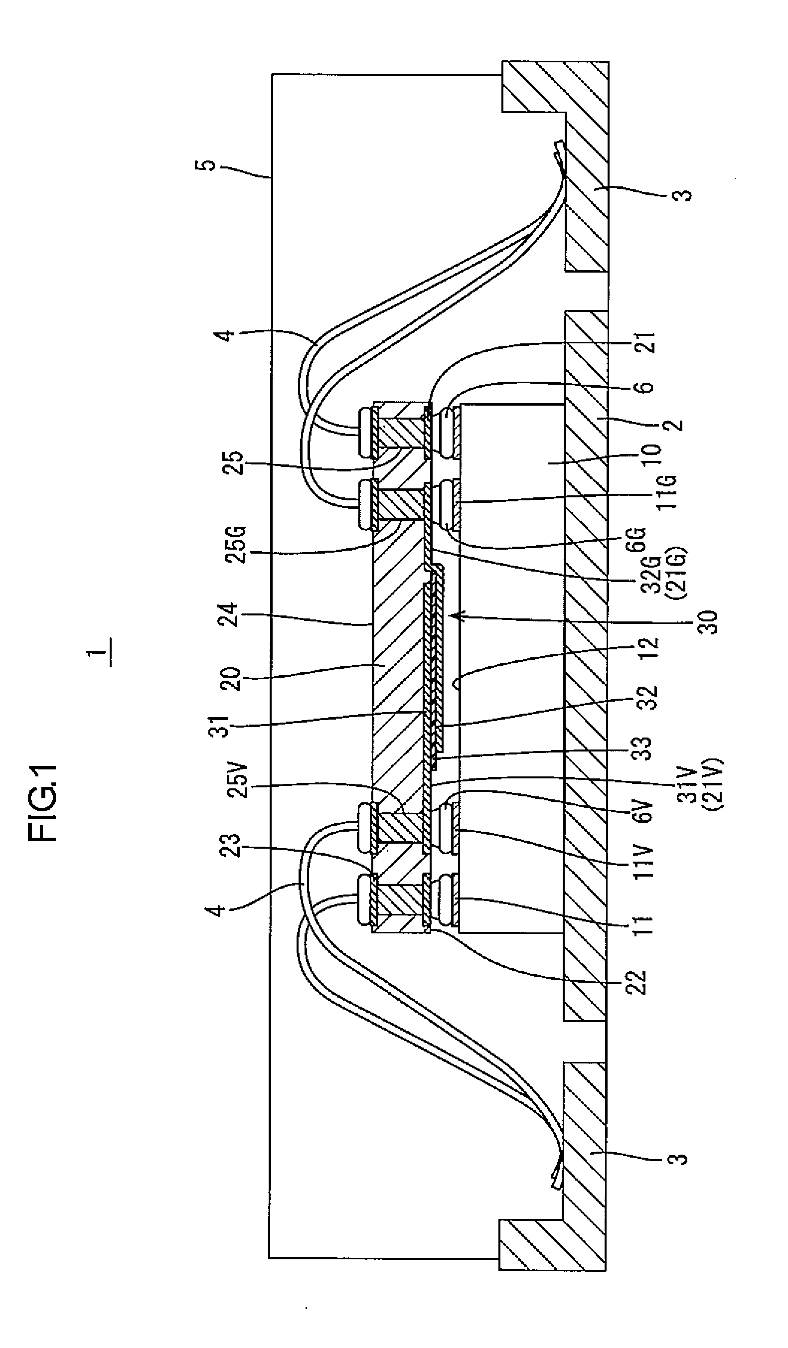
[0055]A second embodiment will now be described with reference to FIG. 6 to FIG. 11. Members similar to those of the first embodiment will be designated with similar signs and their description will be omitted. Accordingly, only differences from the first embodiment will be described.

[0056]A semiconductor device 1A according to the second embodiment, as illustrated in FIG. 6, differs from the semiconductor device 1 of the first embodiment only in the capacitor disposed on the intermediate substrate 20. Specifically, in the semiconductor device 1A, in addition to the thin-film capacitor 30 of the semiconductor device 1, a multi-layer ceramic capacitor (an example of “chip capacitor”) 40 is disposed on the intermediate substrate 20. The chip capacitor is not limited to the multi-layer ceramic capacitor (MLCC).

[0057]The multi-layer ceramic capacitor 40 is formed on the external connection surface 24 of the i...


PUM


Abstract

A semiconductor device is provided with: a semiconductor chip die-bonding mounted face up on a support; an intermediate substrate connecting the semiconductor chip to a plurality of external connection portions; and a plurality of connection bumps connecting the semiconductor chip and the intermediate substrate. The plurality of connection bumps includes a plurality of power supply bumps connected to a plurality of electrode pads on the semiconductor chip for supplying power to the semiconductor chip. The intermediate substrate includes: a plurality of power supply pads connected to the plurality of electrode pads through the plurality of power supply bumps; a bump surface facing the semiconductor chip and having a plurality of power supply pads formed thereon; an external connection surface having a plurality of external connection pads formed thereon connected to the external connection portions; and a capacitor connected to the plurality of power supply bumps.

Description

TECHNICAL FIELD[0001]The present invention relates to a semiconductor device, and more particularly, to a semiconductor device provided with a semiconductor chip die-bonded face up to a support and with a capacitor.BACKGROUND ART[0002]Conventionally, as a semiconductor device of the above type, the technology disclosed in Patent Document 1, for example, is known. In Patent Document 1, as shown in FIG. 1 thereof, onto a lower-tier chip 7 as a support, an upper-tier chip 2 as a semiconductor chip is die-bonded face up. In the semiconductor device 1, the upper chip 2 and passive chip components 3 mounted around the upper chip 2, such as chip capacitors, are connected via wires 5 and a wiring substrate 4, for example.[0003]Patent Document 1: Japanese Unexamined Patent Publication No. 2004-296613[0004]However, as the clock frequency of semiconductor chips (LSI) has increased in recent years, when the wiring distance from the LSI to a capacitor is large, the high frequency impedance due t...

Claims


Application Information

Patent Timeline
Patent Type & Authority Applications(United States)
IPC IPC(8): H01L23/00H01L23/495H01G4/228H01G4/40H01L23/31H01L23/498H01G4/33
CPCH01L24/17H01L23/49838H01L24/06H01L23/49541H01G4/33H01G4/40H01L2924/19107H01L23/3114H01G4/228H01L2224/16227H01L2224/0401H01L2924/19041H01L2924/19102H01L23/49827H01L24/10H01L2224/12105H01L25/00H01L2924/181H01L24/16H01L2224/16225H01L2224/1308H01L23/49531H01L23/50H01L24/13H01L2224/13101H01L2224/13144H01L2924/19015H01L2924/19106H01L23/49551H01G4/30H01G2/065H01L2924/00012H01L2924/00014H01L2924/014H01L23/32H01L23/12H01L2224/73
Inventor HATTORI, ATSUNORI
Owner NODA SCREEN
Why Eureka
Try Eureka