

Developing apparatus, developing method and storage medium
a technology of developing apparatus and development method, applied in the field of developing apparatus, can solve the problems of inability to solve the foregoing problem, deterioration of the critical dimension uniformity of the cpu (critical dimension) of the cd (critical dimension) in one exposure region (shot) within the wafer plane, and fluctuation in reaction, so as to improve the line-width uniformity of the resist pattern, improve the developer concentration uniformity, and improve the line-width uniformity within the plan
- Summary
- Abstract
- Description
- Claims
- Application Information
AI Technical Summary
Benefits of technology
Problems solved by technology
Method used
Image

Examples
first embodiment
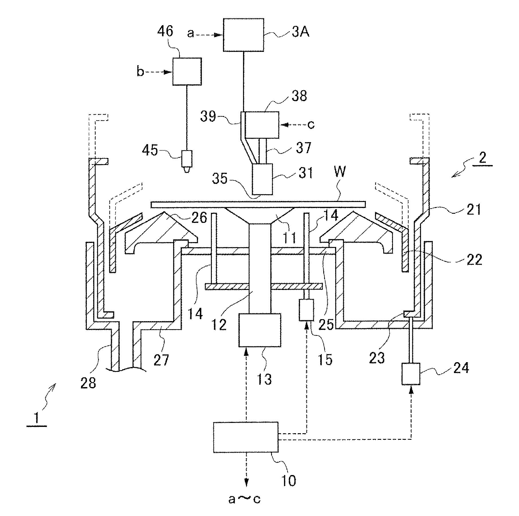
[0071]FIGS. 1 and 2 show a developing apparatus 1 according to a first embodiment of the present invention. A wafer W having a resist film formed on its surface is transferred to the developing apparatus 1 and is processed therein. The resist film has been exposed with a predetermined pattern. The developing apparatus 1 includes a spin chuck 11 serving as a substrate holder. The spin chuck 11 is configured to absorb (suck) a central portion of the rear surface of the wafer W such that the wafer W is held horizontally. The spin chuck 11 is connected to a rotating and driving unit 13 disposed below through a rotating shaft 12.
[0072]The developing apparatus 1 is provided with a cup body 2 which surrounds the wafer W held by the spin chuck 11. The cup body 2 is composed of an outer cup 21 and an inner cup 22. An upper side of the cup body 2 is opened. An upper part of the outer cup body 21 has a rectangular shape, while a lower part thereof has a cylindrical shape. The reference number ...
second embodiment
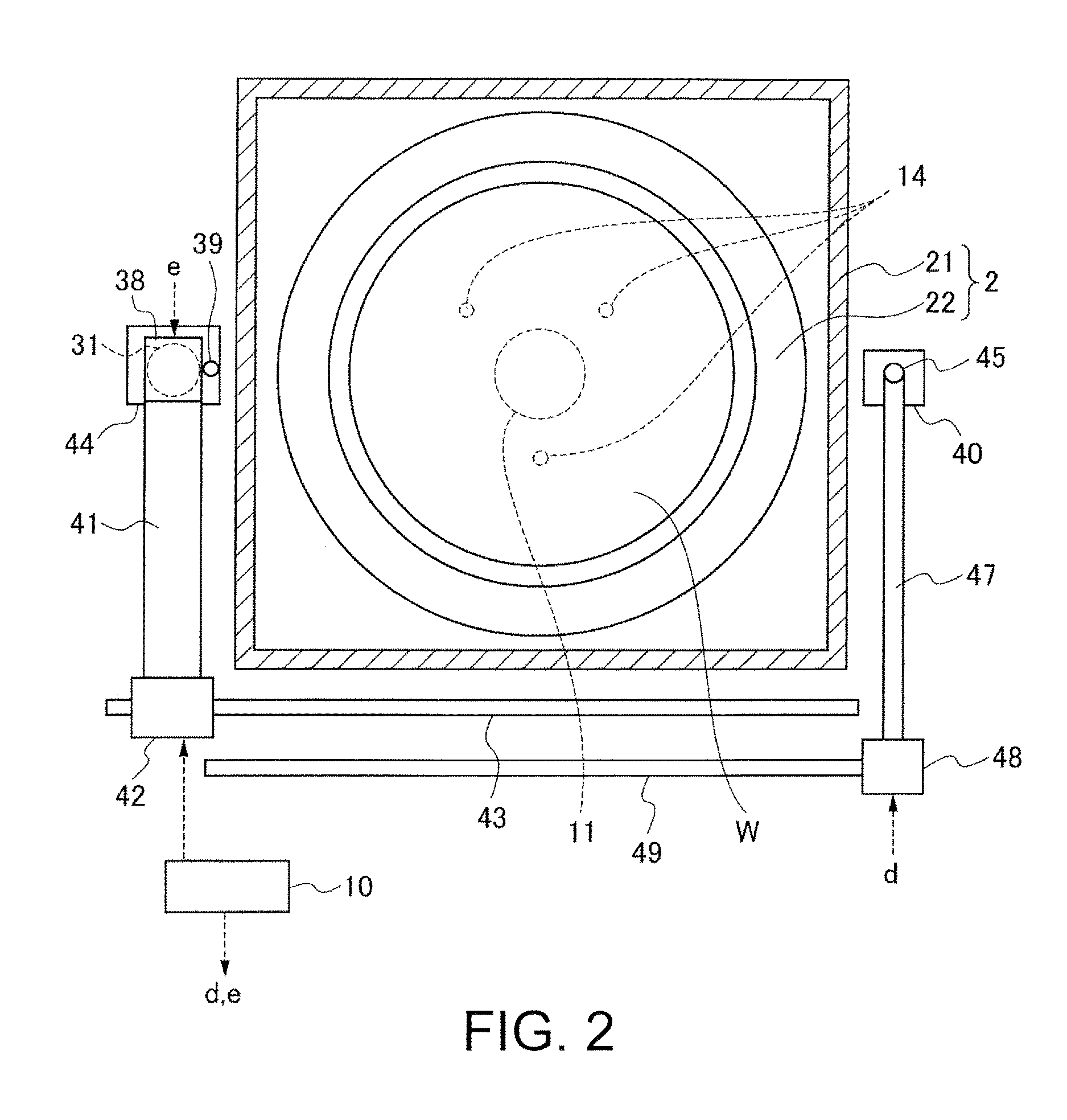
[0102]Next a second embodiment is described, focusing on the differences from the first embodiment. FIG. 18 is a plan view showing a developing apparatus 5 used in the second embodiment. The developing apparatus 5 differs from the developing apparatus 1 in that the two developer nozzles 31 are provided. The developer supply pipe 39, the arm 41, the moving mechanism 42, the guide rail 43 and the waiting area 44 are provided for each of the developer nozzles 31. Thus, the rotation, the discharge of the developer and the movement in the radial direction of the wafer W can be independently performed by each developer nozzle 31. For the convenience of explanation, these developer nozzles 31 are shown by the first developer nozzle 31A and the second developer nozzle 31B.
[0103]A developing process in the second embodiment is explained with reference to the operational views of the developing apparatus 5 shown in FIGS. 19 to 22 and the time chart shown in FIG. 23. Similarly to FIG. 15, the ...
third embodiment
[0110]Next, a third embodiment is described. In the third embodiment, the developing apparatus 5 explained in the second embodiment is used. A developing process in the third embodiment is explained with reference to the operation diagrams of the developing apparatus 5 shown in FIGS. 25 to 28. Similarly to the second embodiment, a time chart of FIG. 29 shows the rotating speed of the wafer W in the developing process in the third embodiment, the rotating speeds of the respective developer nozzles, the discharge time periods of the developer and the moving time periods of the respective developer nozzles.
[0111]The first developer nozzle 31A is located above the central portion of the wafer W, and the second developer nozzle 31B is located above the peripheral portion of the wafer W, respectively, and they are lowered to come close to the wafer W (FIG. 25). The developer is discharged respectively from the first developer nozzle 31A and the second developer nozzle 31B, and the develop...
PUM
| Property | Measurement | Unit |
|---|---|---|
| diameter | aaaaa | aaaaa |
| distance | aaaaa | aaaaa |
| diameter d1 | aaaaa | aaaaa |
Abstract
Description
Claims
Application Information