Array substrate, manufacturing method thereof, and display device

The technology of an array substrate and a manufacturing method, which is applied in the field of array substrate manufacturing, can solve the problem of increasing the coupling capacitance between the data line 4 and the common electrode line, adverse effects, increasing the coupling capacitance between the data line and the common electrode line or the data line and the scanning line, etc. question

Active Publication Date: 2017-10-13
HEFEI XINSHENG OPTOELECTRONICS TECH CO LTD +1
View PDF3 Cites 0 Cited by
  • Summary
  • Abstract
  • Description
  • Claims
  • Application Information

AI Technical Summary

Problems solved by technology

[0004] In the prior art, the design of increasing the line width of the jumper on the mask plate is adopted, but this method will increase the coupling capacitance between the data line and the common electrode line or between the data line and the scanning line, for example figure 2 As shown, the data line 4 formed at the bridge is wider than the data line 4 at other positions, which increases the coupling capacitance between the data line 4 and the common electrode line 3, and still has adverse effects

Method used


Image

  • Array substrate, manufacturing method thereof, and display device
  • Array substrate, manufacturing method thereof, and display device
  • Array substrate, manufacturing method thereof, and display device

Examples


Embodiment 1

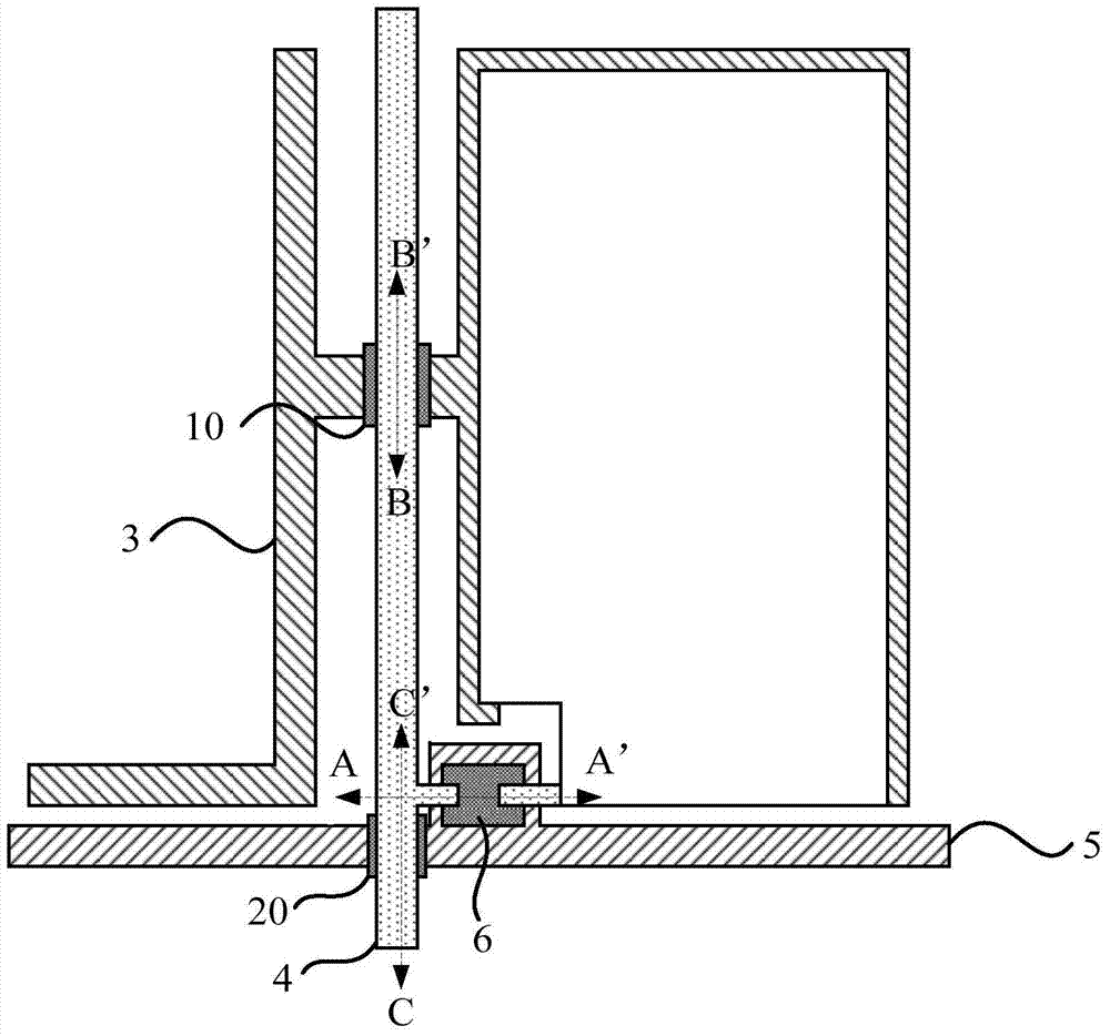
[0073] Such as image 3 As shown, the array substrate according to one embodiment of the present invention includes:

[0074] base1;

[0075] Gate lines 5, common electrode lines 3 and data lines 4 arranged on the substrate;

[0076] The first spacer layer 10 disposed in the first overlapping area of ​​the common electrode line 3 and the data line 4 and located between the common electrode line 3 and the data line 4, the first spacer layer 10 extends at least in the width direction of the data line 4 One side is extended to a preset length;

[0077] and / or

[0078] The second spacer layer 20 arranged in the second overlapping area of ​​the gate line 5 and the data line 4, and between the gate line and the data line 4, the second spacer layer 20 in the second overlapping area is in the width direction of the data line 4 The top extends to at least one side for a preset length.

[0079] The first spacer layer 10 can increase the distance between the common electrode line ...

Embodiment 2

[0091] Such as Figure 7 As shown, preferably, according to yet another embodiment of the present invention, the array substrate further includes:

[0092] a gate 2 disposed on the substrate 1,

[0093] The second spacer layer 20 is also arranged in the third overlapping area between the gate 2 and the data line 4, and is located between the gate 2 and the data line 4,

[0094] The second spacer layer 20 in the third overlapping region extends to at least one side in the width direction of the data line 4 by a predetermined length.

[0095] Compare Figure 7 with image 3 It can be seen that there is an overlapping area between the gate 2 and the data line 4 in the second embodiment, which is intuitively expressed as Figure 7 The gate 2 in the ratio image 3 The gate 2 is large, not only located under the active layer 6, but also located under the data line 4, the specific cross-sectional view is as follows Figure 9 shown.

[0096] Since multiple pixel areas in the ar...


PUM


Abstract

The present invention relates to an array substrate, a manufacturing method thereof, and a display device. The array substrate includes: gate lines, common electrode lines, and data lines disposed on a substrate; The first spacer layer between the common electrode line and the data line, the first spacer layer extends to at least one side in the width direction of the data line for a predetermined length; and / or is arranged in the overlapping area of ​​the gate line and the data line, and is located A second spacer layer between the gate line and the data line, the second spacer layer extends to at least one side in the width direction of the data line for a predetermined length. By setting the first spacer layer and / or the second spacer layer, when exposing the data line metal layer, the data caused by the difference in light reflectance between the common electrode layer metal and / or the gate line layer metal and the data line layer metal can be reduced. The difference in line width can improve the uniformity of data line width, reduce the risk of data line disconnection, and improve product yield.

Description

technical field [0001] The present invention relates to the field of display technology, in particular, to an array substrate, a display device and a manufacturing method of the array substrate. Background technique [0002] TFT (Thin Film Field Effect Transistor) driven display devices are currently the mainstream technology in the display field. A thin film field effect transistor display usually includes a color filter substrate and a TFT array substrate. The TFT array substrate includes a plurality of pixel units, and each pixel unit corresponds to a TFT. When a certain voltage is applied to the gate of the TFT, when the gate voltage reaches the threshold voltage, the channel is turned on (that is, the active layer is turned on), thereby turning on the source and drain, and the signal in the data line is transmitted to the TFT through the source. The drain, and further controls the pixel electrode electrically connected to the drain. The voltage difference between the ...

Claims


Application Information

Patent Timeline
Patent Type & Authority Patents(China)
IPC IPC(8): G02F1/1362
CPCG02F1/136286G02F1/136295H01L27/1222H01L27/124H01L27/127
Inventor 马骏
Owner HEFEI XINSHENG OPTOELECTRONICS TECH CO LTD
Why Eureka
Try Eureka