Semiconductor structure and forming method thereof

A semiconductor and pattern structure technology, applied in semiconductor/solid-state device manufacturing, optics, instruments, etc., can solve the problems of increasing the difficulty and complexity of integrated circuits, improve the uniformity and controllability of the effect, and improve the uniformity of the line width. , Improve the effect of local line width uniformity

Pending Publication Date: 2022-02-22
SEMICON MFG INT (SHANGHAI) CORP +1
View PDF0 Cites 0 Cited by
  • Summary
  • Abstract
  • Description
  • Claims
  • Application Information

AI Technical Summary

Problems solved by technology

[0003] During the development of integrated circuits, usually while the functional density (that is, the number of interconnection structures per chip) gradually increases, the geometric size (that is, the minimum component size that can be produced using process steps) gradually decreases, which increases accordingly. Difficulty and complexity of integrated circuit manufacturing
[0004] At present, in the case of shrinking technology nodes, how to improve the matching degree between the pattern formed on the wafer and the target pattern has become a challenge

Method used


Image

  • Semiconductor structure and forming method thereof
  • Semiconductor structure and forming method thereof
  • Semiconductor structure and forming method thereof

Examples


Embodiment Construction

[0014] Graphics transfers currently have poor precision. The reason for the poor accuracy of pattern transfer is now analyzed in combination with a method for forming a semiconductor structure.

[0015] Figure 1 to Figure 6 It is a structural schematic diagram corresponding to each step in a method for forming a semiconductor structure.

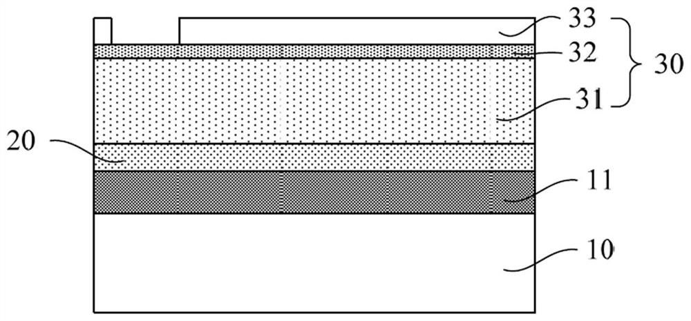
[0016] refer to figure 1 A substrate 10 is provided, and a hard mask material layer 11 and a material layer 20 to be doped located on the hard mask material layer 11 are formed on the substrate 10 .

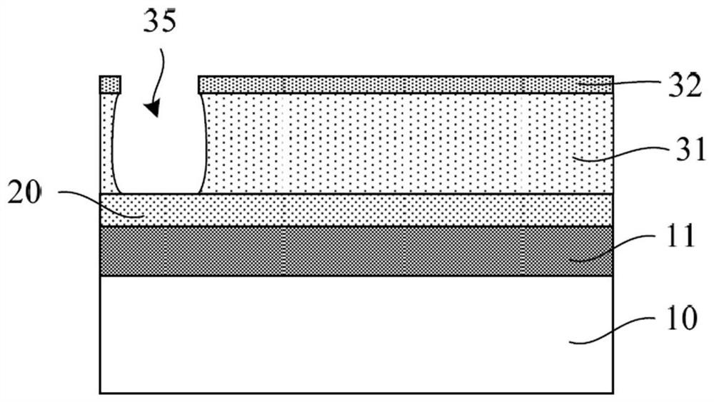
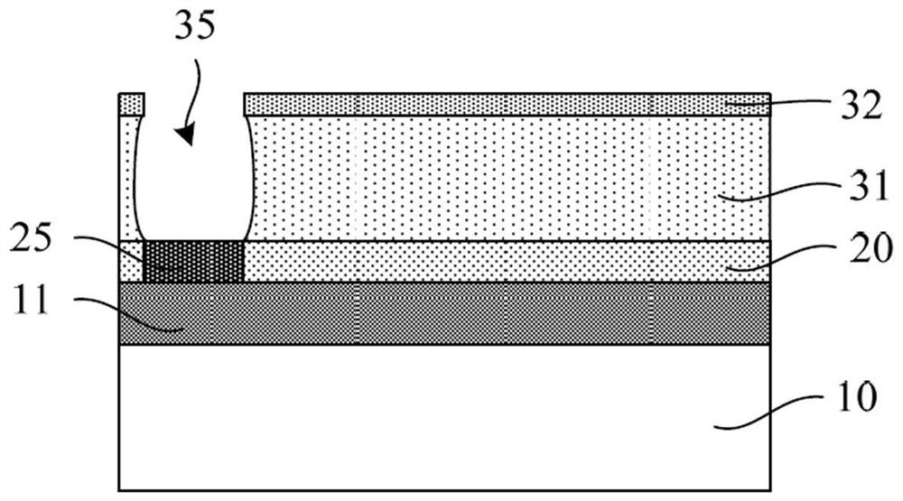
[0017] combined reference Figure 1 to Figure 4 , performing doping treatment on the material layer 20 to be doped.

[0018] Specifically, the doping treatment includes:

[0019] like figure 1 As shown, a pattern structure layer 30 is formed on the material layer 20 to be doped, and the pattern structure layer 30 includes a planarization layer 31, an anti-reflection coating 32 and a patterned photoresist stacked sequentially from bottom ...


PUM

PropertyMeasurementUnit
angleaaaaaaaaaa

Abstract

The invention discloses a semiconductor structure and a forming method thereof. The forming method comprises the steps of providing a substrate; forming a to-be-doped material layer and a top hard mask layer located on the to-be-doped material layer on the substrate; performing one or more patterning processing on the top hard mask layer, the patterning processing comprising: forming a pattern structure layer on the top hard mask layer; etching the top hard mask layer by taking the graphic structure layer as a mask to form a mask opening; and removing the pattern structure layer; and after the last time of patterning processing is completed, doping ions into the to-be-doped material layer exposed out of the mask opening, and taking the to-be-doped material layer doped with ions as a target pattern layer. The etching resistance of the top hard mask layer is high, so that in the process of forming the mask opening, the influence of transverse etching on the side wall of the mask opening is small, the perpendicularity and flatness of the side wall of the mask opening are improved, the line width uniformity of the target pattern layer is correspondingly improved, and the pattern transmission precision is further improved.

Description

technical field [0001] Embodiments of the present invention relate to the field of semiconductor manufacturing, and in particular, to a semiconductor structure and a method for forming the same. Background technique [0002] With the rapid growth of the semiconductor integrated circuit (integrated circuit, IC) industry, semiconductor technology continues to move towards smaller process nodes driven by Moore's Law, making integrated circuits smaller in size, higher in circuit precision, and development in the direction of higher complexity. [0003] During the development of integrated circuits, usually while the functional density (that is, the number of interconnection structures per chip) gradually increases, the geometric size (that is, the minimum component size that can be produced using process steps) gradually decreases, which increases accordingly. Difficulty and complexity of integrated circuit fabrication. [0004] At present, how to improve the matching degree b...

Claims


Application Information

Patent Timeline
Patent Type & Authority Applications(China)
IPC IPC(8): H01L21/027H01L21/033G03F1/46G03F1/80
CPCH01L21/0276H01L21/0337H01L21/0338G03F1/46G03F1/80
Inventor 郑二虎王兆龙胡敏达
Owner SEMICON MFG INT (SHANGHAI) CORP
Why Eureka
Try Eureka