Formation method of semiconductor structure

A semiconductor and graphics technology, applied in the direction of semiconductor devices, semiconductor/solid-state device manufacturing, electrical components, etc., can solve the problems of increasing the difficulty and complexity of integrated circuits, improve the problem of serious lateral diffusion, improve the verticality of side walls and Line width accuracy, the effect of improving accuracy

Pending Publication Date: 2022-05-13
SEMICON MFG INT (SHANGHAI) CORP +1
View PDF0 Cites 0 Cited by
  • Summary
  • Abstract
  • Description
  • Claims
  • Application Information

AI Technical Summary

Problems solved by technology

[0003] During the development of integrated circuits, usually while the functional density (that is, the number of interconnection structures per chip) gradually increases, the geometric size (that is, the minimum component size that can be produced using process steps) gradually decreases, which increases accordingly. Difficulty and complexity of integrated circuit manufacturing
[0004] At present, how to improve the accuracy of graphics transfer has become a challenge in the case of shrinking technology nodes

Method used


Image

  • Formation method of semiconductor structure
  • Formation method of semiconductor structure
  • Formation method of semiconductor structure

Examples


Embodiment Construction

[0031] At present, the electrical performance and reliability of the device still need to be improved. Combining with the formation method of a semiconductor structure, the reasons why its electrical performance and reliability still need to be improved are analyzed.

[0032] refer to Figure 1 to Figure 4 , shows a structural schematic diagram corresponding to each step in a method for forming a semiconductor structure.

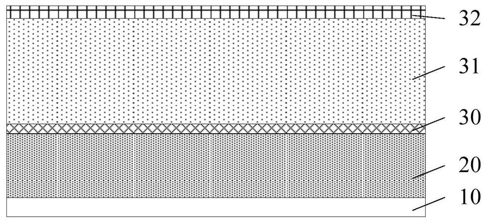
[0033] refer to figure 1 , providing a substrate 10, on which a pattern transfer material layer 20 is formed; an etch stop layer 30 is formed on the pattern transfer material layer 20; a mask layer 31 is formed on the etch stop layer 30; An anti-reflection coating 32 is formed on the mask layer 31 .

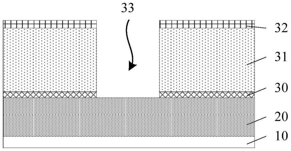
[0034] refer to figure 2 , using a patterning process to form an opening 33 in the mask layer 31 , and the opening 33 runs through the etching stop layer 30 , the mask layer 31 and the anti-reflection coating 32 .

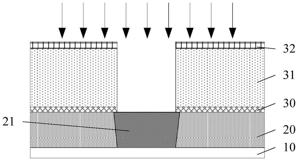
[0035] refer to image 3 , forming the...


PUM

PropertyMeasurementUnit
thicknessaaaaaaaaaa
thicknessaaaaaaaaaa

Abstract

A method for forming a semiconductor structure comprises the following steps: providing a substrate on which a pattern transfer material layer is formed; forming a mask layer on the pattern transfer material layer, wherein an opening penetrating through the mask layer is formed in the mask layer; forming a side wall layer on the side wall of the opening; with the side wall layer as a mask, first ion implantation is carried out on the pattern transfer material layer at the bottom of the opening, target ions are implanted into the pattern transfer material layer, a pattern layer penetrating through the pattern transfer material layer is formed, and the target ions are used for improving the etching selection ratio between the material transfer layer and the pattern layer; and after the pattern layer is formed, removing the mask layer and the side wall layer. According to the invention, the side wall layer is formed at the opening, the target ion concentration at each position of the pattern layer can easily meet the process requirement in the direction of the thickness of the pattern layer, and meanwhile, the problem of serious transverse diffusion of the target ions at the position close to the bottom of the opening is improved, so that the side wall perpendicularity and the line width precision of the pattern layer can be improved; and therefore, the pattern transmission precision is improved.

Description

technical field [0001] Embodiments of the present invention relate to the field of semiconductor manufacturing, and in particular, to a method for forming a semiconductor structure. Background technique [0002] With the rapid growth of the semiconductor integrated circuit (integrated circuit, IC) industry, semiconductor technology continues to move towards smaller process nodes driven by Moore's Law, making integrated circuits smaller in size, higher in circuit precision, and development in the direction of higher complexity. [0003] During the development of integrated circuits, usually while the functional density (that is, the number of interconnection structures per chip) gradually increases, the geometric size (that is, the minimum component size that can be produced using process steps) gradually decreases, which increases accordingly. Difficulty and complexity of integrated circuit fabrication. [0004] At present, how to improve the accuracy of graphics transfer ...

Claims


Application Information

Patent Timeline
Patent Type & Authority Applications(China)
IPC IPC(8): H01L21/027H01L21/033H01L21/336
CPCH01L21/0276H01L21/0338H01L29/66803
Inventor 赵猛
Owner SEMICON MFG INT (SHANGHAI) CORP
Why Eureka
Try Eureka