Bonded structure, piezoelectric device, liquid ejecting head, and method of manufacturing bonded structure

a piezoelectric device and ejector technology, applied in the direction of piezoelectric/electrostrictive/magnetostrictive devices, printing, electrical equipment, etc., can solve the problems of deformation or breakage of the bump, the bonding force between the substrates after bonding deterioration, and the shape of the bump is deformed or broken, so as to achieve the effect of convenient manufacturing

Active Publication Date: 2017-02-23
SEIKO EPSON CORP
View PDF1 Cites 3 Cited by
  • Summary
  • Abstract
  • Description
  • Claims
  • Application Information

AI Technical Summary

Benefits of technology

[0023]According to the method, the hardness of the photosensitive adhesive layer in the first region and the photosensitive adhesive lay

Problems solved by technology

When the first substrate and the second substrate are bonded to each other, if the photosensitive adhesive before bonding is excessively hard, there is a concern that a bonding force between both the substrates after bonding is deteriorated.
Meanwhile, if the photosensitive adhesive before bonding is excessively soft, there is a concern that pressure is focused on the

Method used


Image

  • Bonded structure, piezoelectric device, liquid ejecting head, and method of manufacturing bonded structure
  • Bonded structure, piezoelectric device, liquid ejecting head, and method of manufacturing bonded structure
  • Bonded structure, piezoelectric device, liquid ejecting head, and method of manufacturing bonded structure

Examples


second embodiment

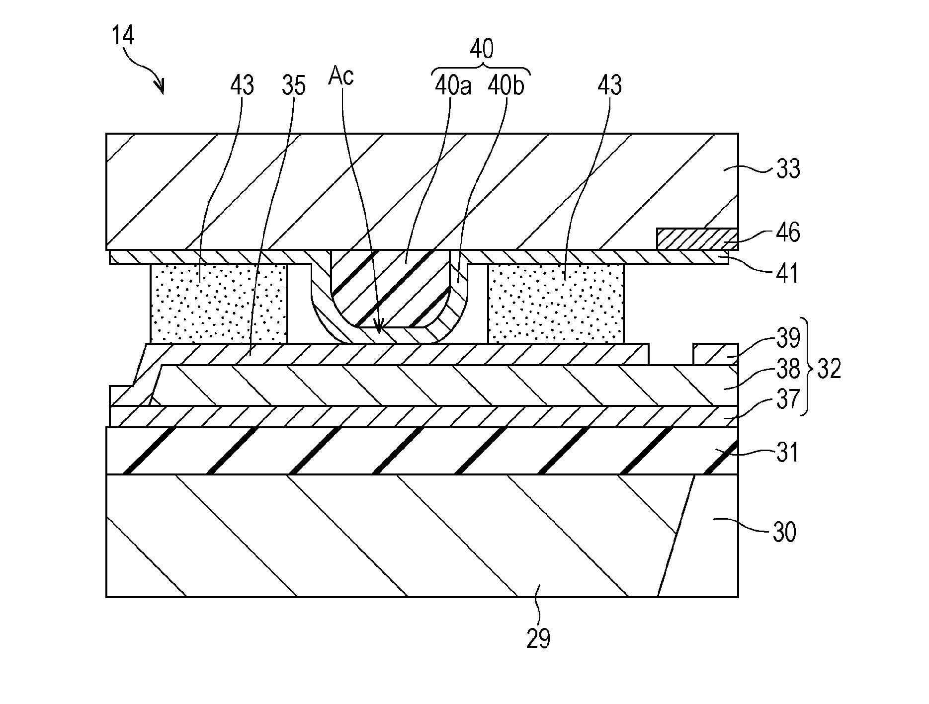
[0072]The light absorbing film 44 is formed on the second region A2 as described above, in the exposing and developing process after forming the photosensitive adhesive layer 43′, as illustrated in FIG. 8B, and the photosensitive adhesive 43 which has a higher hardness difference can be formed on a different respective position. That is, the photosensitive adhesive 43b in the second region A2 can be further softened than the photosensitive adhesive 43a in the first region A1. Accordingly, a bonding force by the photosensitive adhesive 43b formed on the second region A2 can be further increased, an adhesion force of the silicon single crystal substrate which becomes the sealing plate 33 and the silicon single crystal substrate which becomes the pressure chamber forming substrate 29 can be further increased. Moreover, the other configurations and manufacturing methods are the same as that of the second embodiment, and thus description thereof is omitted.

fourth embodiment

[0073]Further, in each embodiment described above, a region in which the light is reflected by the driving wiring 41 or the lead electrode layer 35, which is a metal layer, is set to the first region A1; however, it is not limited thereto. Without using a wiring of the driving wiring 41, the lead electrode layer 35, or the like, a metal layer for reflecting light may be separately formed. For example, in a fourth embodiment illustrated in FIG. 9 to FIG. 10B, metal layers for reflecting 47 are formed on a region overlapping the photosensitive adhesive 43 which is formed on one side (piezoelectric element 32 side) of the resin core bump 40 in a region overlapping the photosensitive adhesive 43 on the pressure chamber forming substrate 29 side. In the embodiment, the region on which the metal layers for reflecting 47 are formed and the region on which the lead electrode layer 35 is formed become the first region A1. Moreover, the piezoelectric device 14 in the embodiment is formed when...


PUM


Abstract

Provided is a bonded structure including a first substrate in which a resin portion made of an elastic member protrudes on one surface and a first electrode layer is formed to cover at least a part of the resin portion, and a second substrate in which a second electrode layer electrically connected to the first electrode layer is formed on a surface facing the first substrate, the first substrate and the second substrate being bonded to each other in a state in which a photosensitive adhesive is interposed therebetween. In a surface of one of the first substrate and the second substrate on the photosensitive adhesive side, a first region reflecting light and a second region less likely to reflect light than the first region are provided in positions different from each other on a region overlapping the photosensitive adhesive in a substrate bonding direction.

Description

CROSS-REFERENCE TO RELATED APPLICATIONS[0001]The present application claims priority to Japanese Patent Application No. 2015-163473 filed on Aug. 21, 2015, which is hereby incorporated by reference in its entirety.BACKGROUND[0002]1. Technical Field[0003]The present invention relates to a bonded structure including a first substrate in which a first electrode layer is formed and a second substrate in which a second electrode layer electrically connected with the first electrode layer is formed, a piezoelectric device and a liquid ejecting head which include the bonded structure, and a method of manufacturing the bonded structure.[0004]2. Related Art[0005]A bonded structure in which a first substrate having a first electrode layer and a second substrate having a second electrode layer are bonded with each other in a state of being electrically connected is built into various electronic devices. For example, a piezoelectric device which is a type of the bonded structure is applied to v...

Claims


Application Information

Patent Timeline
IPC IPC(8): B41J2/14H01L41/27H01L41/297H01L41/047
CPCB41J2/14201H01L41/297H01L41/27H01L41/0471B41J2202/22B41J2/14233B41J2/161B41J2/1623B41J2/1626B41J2/1631B41J2/1632B41J2/1645B41J2002/14362B41J2002/14419B41J2002/14491H10N30/875H10N30/2047H10N30/06H10N30/05H10N30/067H10N30/871
Inventor YOSHIIKE, MASASHI
Owner SEIKO EPSON CORP
Why Eureka
Try Eureka