Display panel with external signal lines under gate drive circuit

a gate drive circuit and display panel technology, applied in the field of display panels, can solve the problems of visual defects, thickness and weight of display panels, and necessitate some compromises in display, and achieve the effect of reducing the aperture ratio discrepancy between the pixel regions

Active Publication Date: 2017-03-02
LG DISPLAY CO LTD
View PDF5 Cites 38 Cited by
  • Summary
  • Abstract
  • Description
  • Claims
  • Application Information

AI Technical Summary

Benefits of technology

[0007]In a display panel, some elements used in relation with a display functionality can be configured to recognize touch inputs on the screen. For instance, integrated circuits (ICs) may be configured to provide signals for operating the display pixels and for sensing the touch inputs. Also, some electrodes and / or conductive layers implementing a storage capacitor in display pixels used for displaying image from the display panel can be configured to serve as a part of a touch sensor. In this way, a display panel with a lighter weight and thinner profile can be manufactured using fewer parts in fewer manufacturing steps. Such configurations can also eliminate or otherwise reduce various undesired side effects, which may result from placing discrete touch sensor components in the display panel.
[0013]The external signal lines may be positioned to extend across under the plurality of shift registers of the GIP circuit that are implemented with a number of TFTs. The external signal lines can be connected to the parts of the GIP circuit via contact holes through the lower planarization layer. The external signal lines routed underneath the GIP circuit may include various clock signal lines, power signal lines (e.g., VSS, VDD), reset signal lines and more. In some embodiments, signal line for transmitting the common voltage signal may be routed in the inactive area under the GIP circuit. Routing at least some of the external signal lines directly under the GIP circuit allows to reduce the bezel size even further.
[0027]The display panel further includes a masking layer, which includes a plurality of data BM sections and a plurality of gate BM sections. In some embodiments, some part of the data BM strip can be asymmetrically arranged from other parts of the same data BM strip, in order to reduce the aperture ratio discrepancy among the pixel regions.

Problems solved by technology

However, placing a separate substrate for sensing touch inputs on the display panel adds to the thickness and the weight of the display panel.
Integrating the touch sensor components within the display panel, however, often necessitates some compromises to be made in the display qualities.
For instance, conductive lines transmitting signals to and from the display regions in the display panel for an implementation of touch-sensing mechanism may generate unwanted parasitic capacitance with other components of the display panel, which may result in visual defects (e.g., irregular tilting angle of liquid crystal molecules, line dim, moiré effects, etc.).
When implementing a touch sensor within a display panel, fine-tuning of both the touch-sensing functionality and the display functionality can be a challenging task.
Among various types of LCD display panels, arrangement of the components for both functionalities can be especially challenging for the in-plane-switching (IPS) type and the fringe-field-switching (FFS) type LCD display panels as the electrodes for generating fields that controls the orientation of the liquid crystal molecules are provided on the same side of the liquid crystal layer.

Method used


Image

  • Display panel with external signal lines under gate drive circuit
  • Display panel with external signal lines under gate drive circuit
  • Display panel with external signal lines under gate drive circuit

Examples


Embodiment Construction

[0049]Reference will now be made in detail to the exemplary embodiments of the present invention, examples of which are illustrated in the accompanying drawings. Wherever possible, the same reference numbers will be used throughout the drawings to refer to the same or like parts.

[0050]Example embodiments may be described herein with reference to a Cartesian coordinate system in which the x-direction and the y-direction can be equated to the horizontal (row) direction and the vertical (column) direction, respectively. However, one skilled in the art will understand that reference to a particular coordinate system is simply for the purpose of clarity, and does not limit the direction of the structures to a particular direction or a particular coordinate system.

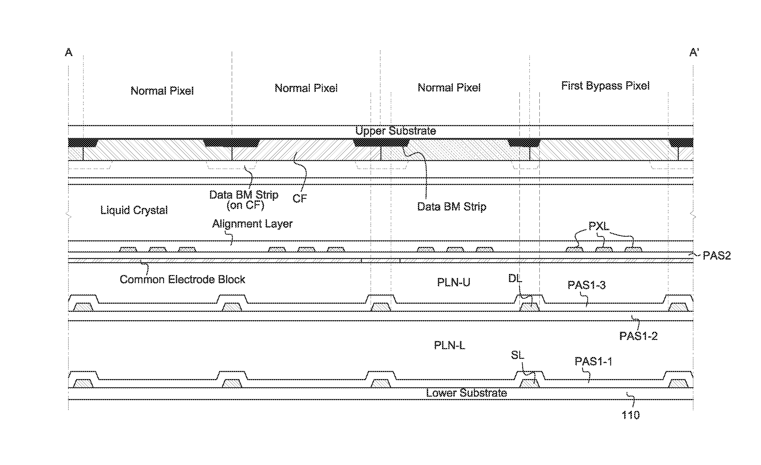
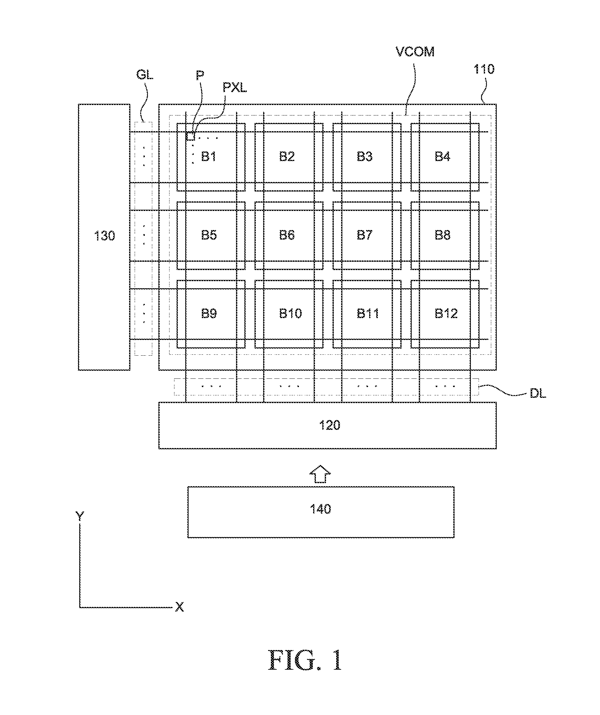
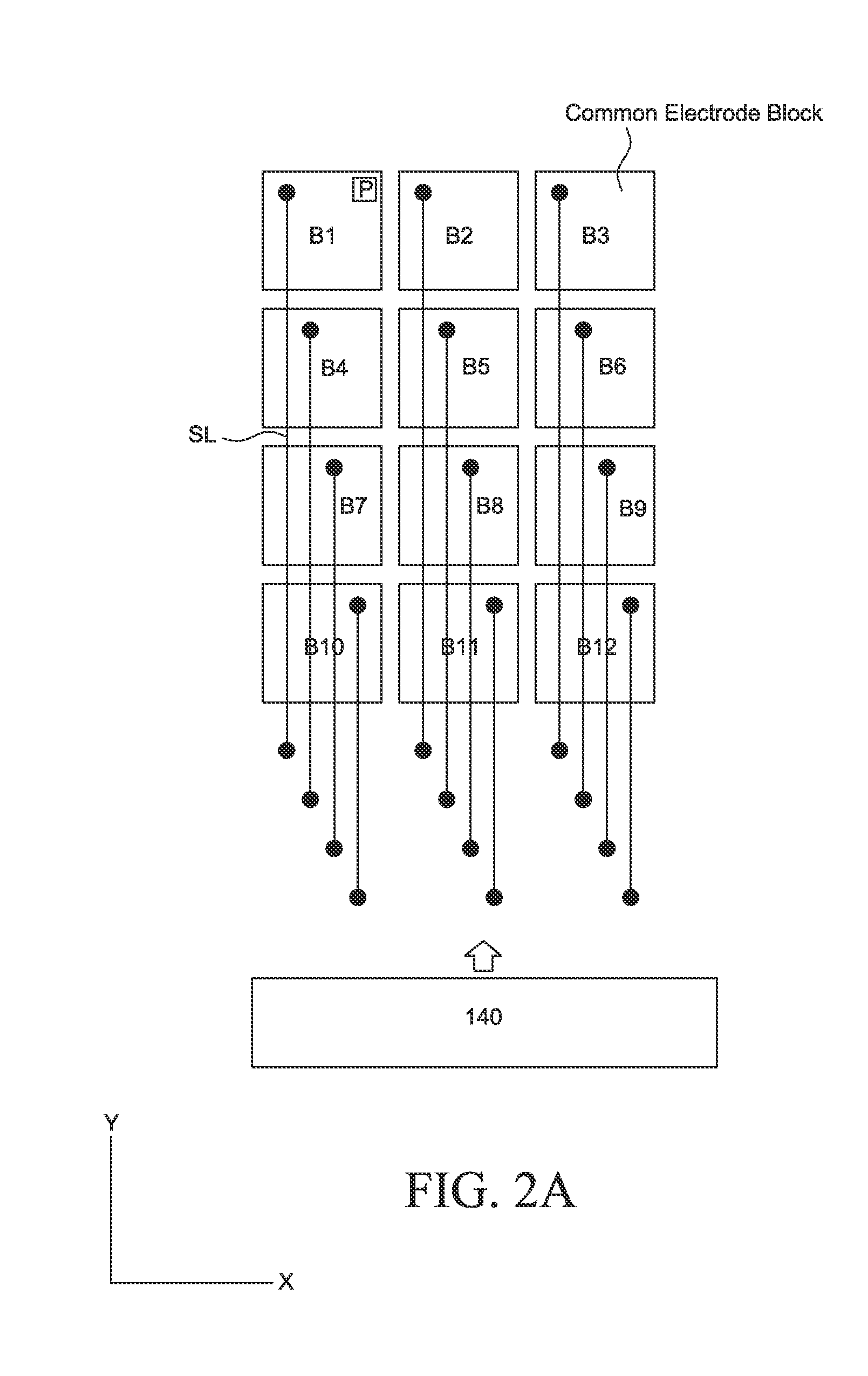
[0051]The following description includes embodiments described in the context of LCDs, in particular the In-Plane-Switching (IPS) mode LCD and the Fringe-Field-Switching (FFS) mode LCD, in which the common electrodes and the pix...


PUM


Abstract

A touch recognition enabled display panel includes a plurality of common electrode blocks serving as touch-sensing regions and / or touch-driving regions. Conductive lines connected to the common electrode blocks are placed under the common electrode blocks and the pixel electrodes of the pixels, and they are routed across the active area, directly toward an inactive area where drive-integrated circuits are located. The conductive lines are positioned under one or more planarization layers, and are connected to the corresponding common electrode blocks via one or more contact holes.

Description

BACKGROUND OF THE INVENTION[0001]Field of the Invention[0002]The present disclosure generally relates to a display panel, and more particularly to a display panel configured for advanced capacitance touch-sensing and a method for manufacturing the same.[0003]Description of the Related Art[0004]A touch screen allows a user to interact with a device simply by touching the graphical interface displayed on the screen with fingers, stylus or other objects. With ease of use and versatility in operation, the touch screen has been one of the most popular user interaction mechanism used in a variety of flat panel displays such as liquid crystal displays (LCDs) and organic light emitting diode (OLED) displays electronic devices.[0005]Conventionally, a substrate with a matrix of touch-driving lines and touch-sensing lines is overlaid on a display panel to provide the touch-sensing functionality. However, placing a separate substrate for sensing touch inputs on the display panel adds to the thi...

Claims


Application Information

Patent Timeline
Patent Type & Authority Applications(United States)
IPC IPC(8): G06F3/041G06F3/044H01L29/24H01L27/12H01L29/786
CPCG06F3/0416H01L27/1225H01L27/124H01L27/1255G06F2203/04103H01L29/24G06F3/0412G06F3/044H01L29/7869H01L27/1248G06F3/0443G06F3/04164G06F3/04166
Inventor KIM, DONGSOOYU, SANGHEEKIM, SANGWOON
Owner LG DISPLAY CO LTD
Why Eureka
Try Eureka