Memory controller

a memory controller and controller technology, applied in the field of memory controllers, can solve the problems of nullifying stealing the cryptographic key by a malicious third party, and unable to ensure the security so as to facilitate the duplication of the data stored in the semiconductor memory

Inactive Publication Date: 2017-03-02
MEGACHIPS
View PDF6 Cites 6 Cited by
  • Summary
  • Abstract
  • Description
  • Claims
  • Application Information

AI Technical Summary

Benefits of technology

[0009]If a third party manages to steal a cryptographic key or password used to access the semiconductor storage apparatus, the third party will be allowed to read all of the data stored in the semiconductor memory, which will enable the third party to easily duplicate the data stored in the semiconductor memory. As a result, illegal duplicates of the semiconductor storage apparatus may be circulated on the market.
[0010]An object of the present invention is to provide a technique that makes it difficult to fabricate an illegal duplicate of a semiconductor storage apparatus.

Problems solved by technology

In implementations where encryption is employed as in the semiconductor memory apparatus of Patent Document 1, a cryptographic key may be stolen by a malicious third party.
If a cryptographic key is stolen, the security of the data stored in the semiconductor memory will be nullified.
In implementations where security is ensured by authentication, a password used for authentication may be stolen, in which case, again, the security of the data stored in the semiconductor memory will be nullified.
As a result, illegal duplicates of the semiconductor storage apparatus may be circulated on the market.
This makes it difficult to fabricate an illegal duplicate of a semiconductor storage apparatus including the memory controller according to the present disclosure.
Since a third party cannot identify the latency-related designated address, the memory controller in an illegal duplicate semiconductor storage apparatus fabricated by the third party cannot transmit the data for the latency-related designated address to the host with the minimum latency.
This makes it difficult to fabricate an illegal duplicate of the semiconductor storage apparatus.
Thus, when the data for the address included in the read command is being transmitted from the memory controller to the host, it is difficult for a third party to identify this data.

Method used


Image

  • Memory controller
  • Memory controller
  • Memory controller

Examples


first embodiment

1. Configuration of Memory System

[0040]{1.1 Overall Configuration}

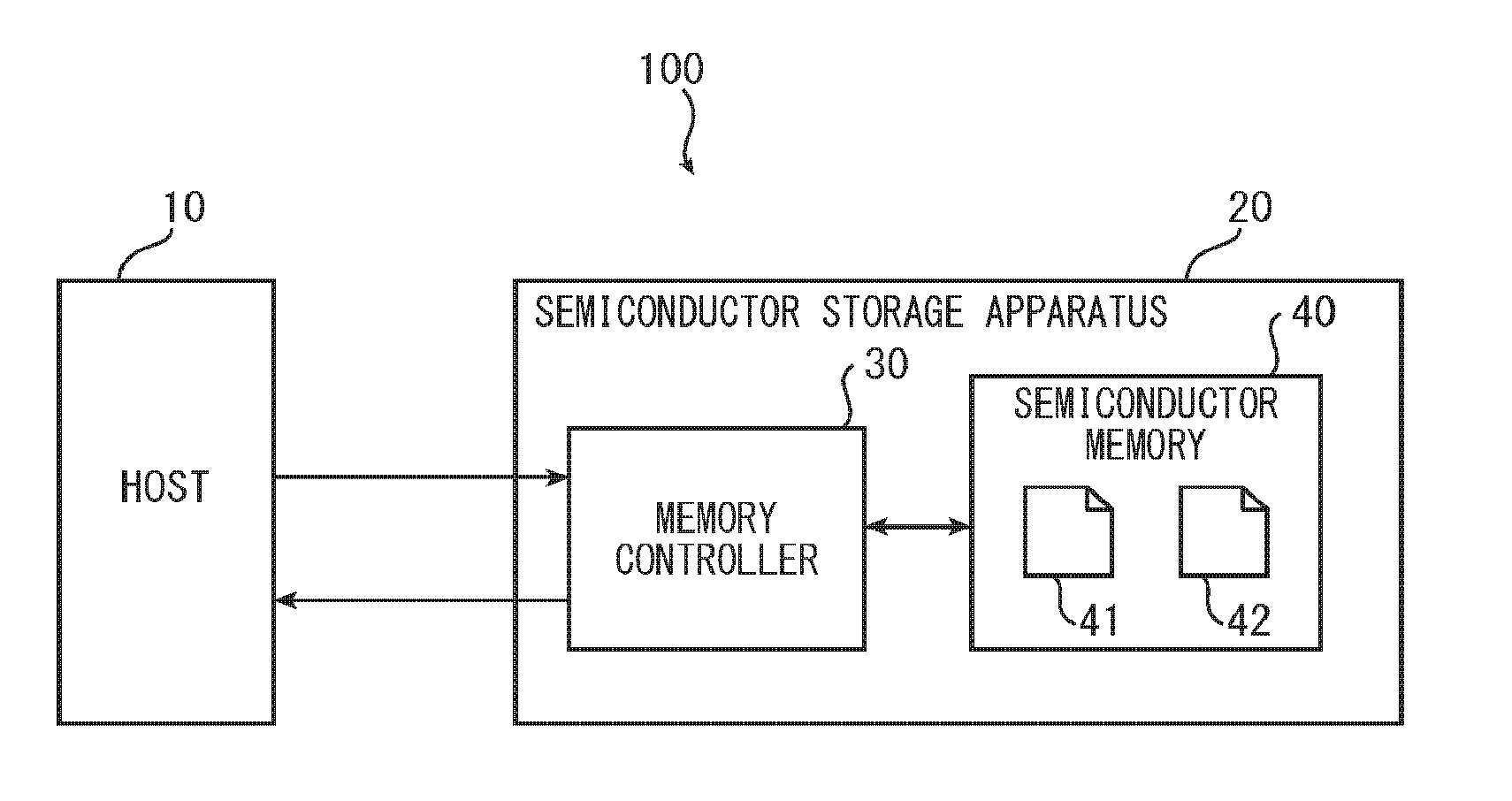
[0041]FIG. 1 is a functional block diagram of a memory system 100 according to a first embodiment of the present invention. As shown in FIG. 1, the memory system 100 includes a host 10 and a semiconductor storage apparatus 20. The semiconductor storage apparatus 20 includes a memory controller 30 and a semiconductor memory 40.

[0042]In response to a request from the host 10, the memory controller 30 accesses the semiconductor memory 40.

[0043]The semiconductor memory 40 is non-volatile, and may be a NAND flash memory, for example. The semiconductor memory 40 stores a program 41 and content data 42 that can be used by the host 10. The program 41 is a program for using the content data 42.

[0044]{1.2 Configuration of Host 10}

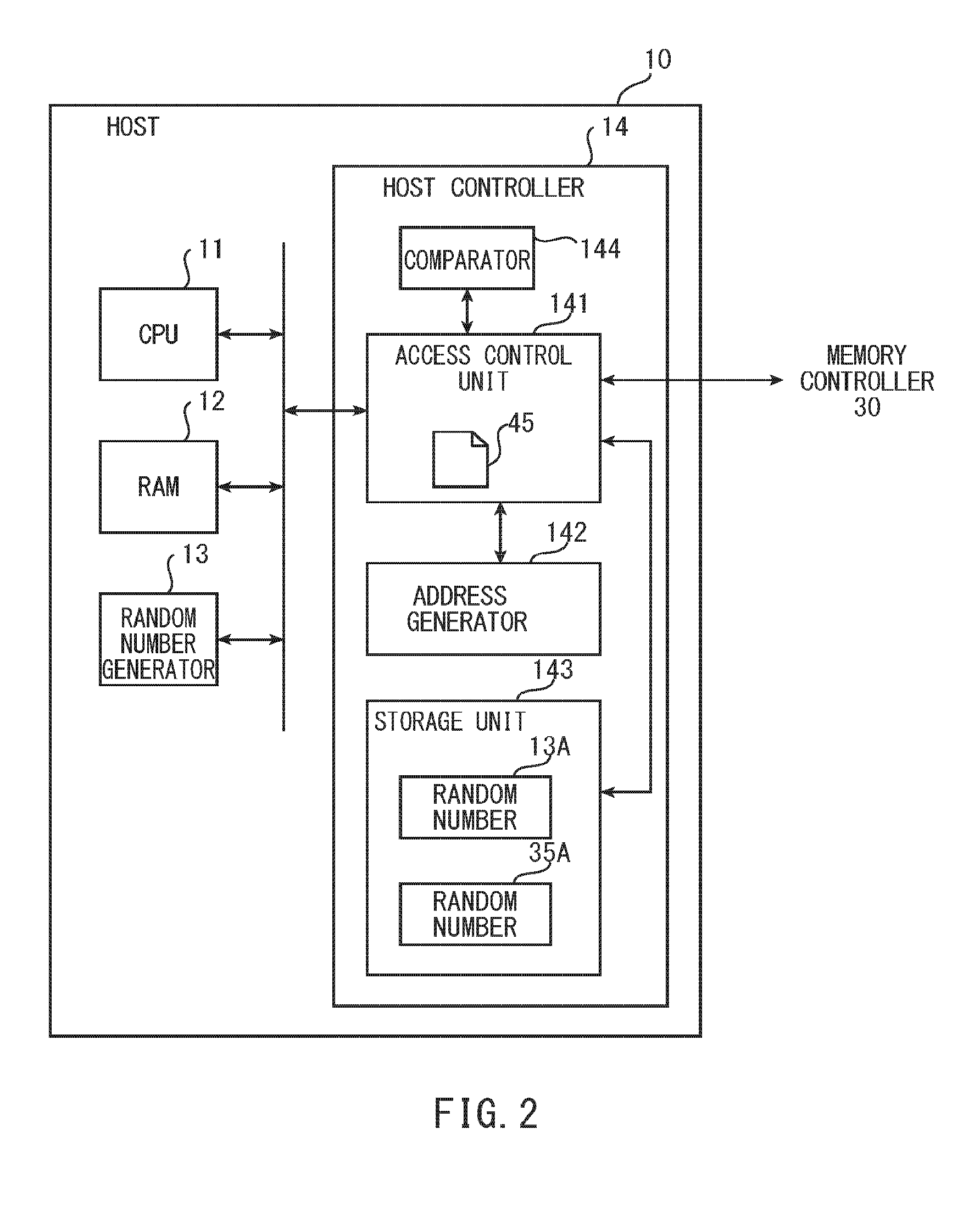
[0045]FIG. 2 is a functional block diagram of the host 10 shown in FIG. 1. As shown in FIG. 2, the host 10 includes a central processing unit (CPU) 11, a random access memory (RAM) 12, a random number ...

second embodiment

1. Configuration of Memory System

[0139]{1.1 Overall Configuration}

[0140]FIG. 12 is a functional block diagram of a memory system 500 according to a second embodiment of the present invention. As shown in FIG. 12, the memory system 500 includes a host 50 and a semiconductor storage apparatus 60. The semiconductor storage apparatus 60 includes a memory controller 70 and a semiconductor memory 80.

[0141]In response to a request from the host 50, the memory controller 70 accesses the semiconductor memory 80.

[0142]The semiconductor memory 80 is non-volatile, and may be a NAND flash memory, for example. The semiconductor memory 80 stores a program 81, content data 82 and specified address data 83. The program 81 is a program for using the content data 82. The specified address data 83 is used to decide whether the memory controller 70 should perform the fixed latency process or variable latency process. The fixed latency process and variable latency process will be described in detail furt...


PUM


Abstract

An object of the present invention is to provide a technique that makes it difficult to fabricate an illegal duplicate of a semiconductor storage apparatus. In a memory controller, an address acquisition unit acquires a latency-related designated address. The latency-related designated address is an address in the semiconductor memory storing data to be transmitted with the minimum latency upon reception of a read command, and is identical with an address held by a host. A pre-acquisition unit reads the data for the latency-related designated address from the semiconductor memory and stores it in the buffer. A comparator compares the address included in the read command to the latency-related designated address. Depending on the result of the comparison by the comparator, a transmission control unit transmits the data stored in the buffer to the host at the time point of completion of a minimum latency.

Description

BACKGROUND[0001]Technical Field[0002]The present invention relates to a memory controller that accesses a semiconductor memory in response to a request by a host.[0003]Description of the Background Art[0004]A semiconductor storage apparatus includes a memory controller and a semiconductor memory such as a NAND flash memory. When the memory controller receives from a host an instruction for reading data, an instruction for writing data or other instructions, the memory controller controls access to the semiconductor memory depending on the instruction from the host.[0005]Traditionally, various measures have been taken to ensure security of data such as content stored in the semiconductor memory, such as authentication or encryption of data. If authentication is employed, the host and memory controller check each other's validity and then read data stored in the semiconductor memory. If encryption is employed, the memory controller encrypts data read from the semiconductor memory and ...

Claims


Application Information

Patent Timeline
Patent Type & Authority Applications(United States)
IPC IPC(8): G06F3/06G06F12/14
CPCG06F3/0623G06F3/0658G06F3/0659G06F2212/214G06F12/14G06F2212/1052G06F3/0679G06F3/0611G06F13/161G06F13/1631
Inventor SUGAHARA, TAKAHIKOYUTANI, HIROMUYOSHIMURA, HAJIME
Owner MEGACHIPS
Why Eureka
Try Eureka