Substrate processing apparatus, method of manufacturing semiconductor device and non-transitory computer-readable recording medium

a processing apparatus and semiconductor technology, applied in the direction of conveyor parts, transportation and packaging, coatings, etc., can solve the problem of reducing productivity and achieve the effect of reducing productivity

Inactive Publication Date: 2017-03-02
KOKUSA ELECTRIC CO LTD
View PDF0 Cites 10 Cited by
  • Summary
  • Abstract
  • Description
  • Claims
  • Application Information

AI Technical Summary

Benefits of technology

[0006]There is a challenge in that productivity is reduced by the mismatch between the numb

Problems solved by technology

There is a challenge in that productivity is reduced by the mismatch between the number

Method used


Image

  • Substrate processing apparatus, method of manufacturing semiconductor device and non-transitory computer-readable recording medium
  • Substrate processing apparatus, method of manufacturing semiconductor device and non-transitory computer-readable recording medium
  • Substrate processing apparatus, method of manufacturing semiconductor device and non-transitory computer-readable recording medium

Examples


first embodiment

[0021]Hereinafter, a first embodiment of the present invention will be described with reference to the drawings.

[0022]Hereinafter, a substrate processing system according to the present embodiment will be described.

[0023](1) Configuration of Substrate Processing System

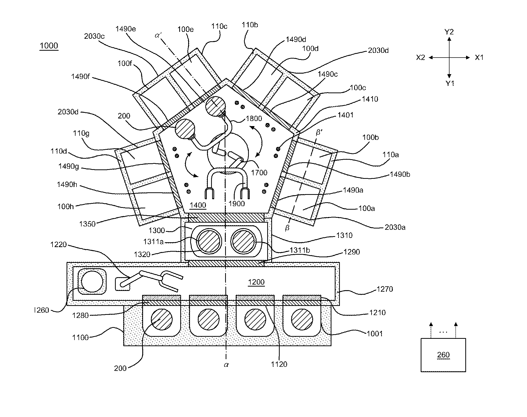
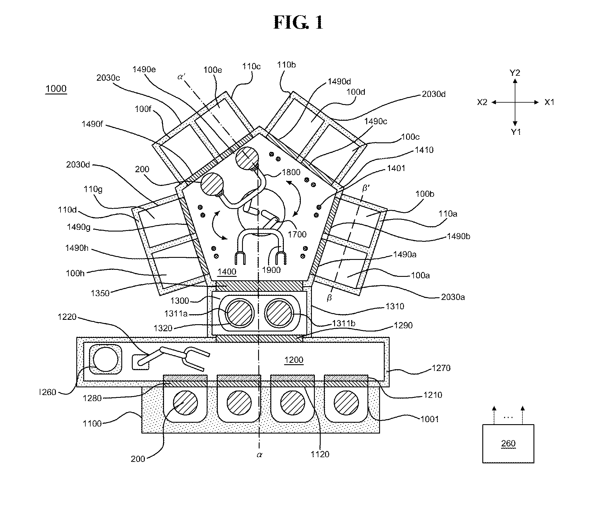
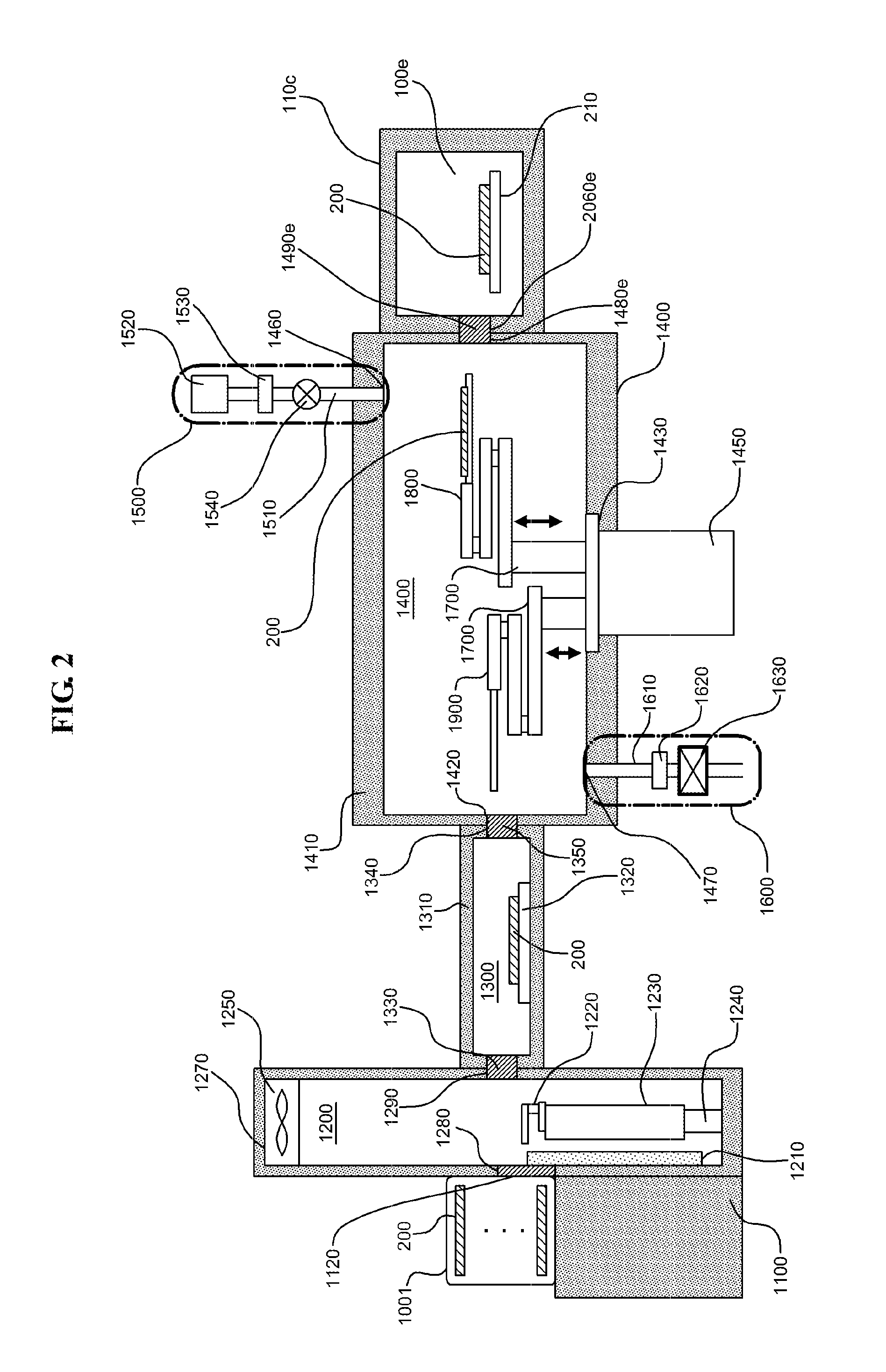
[0024]A configuration of a substrate processing system according to an embodiment of the present invention will be described with reference to FIGS. 1 through 4. FIG. 1 is a cross-sectional view illustrating the configuration of the substrate processing system according to the present embodiment. FIG. 2 is a vertical cross-sectional view taken along line α-α′ of FIG. 1 that illustrates the configuration of the substrate processing system according to the present embodiment. FIG. 3 is an explanatory diagram for describing in detail an arm of FIG. 1. FIG. 4 is a vertical cross-sectional view taken along line β-β′ of FIG. 1 and an explanatory diagram for describing a gas supply system that supplies a gas to a process modu...


PUM

PropertyMeasurementUnit
Flow rateaaaaaaaaaa

Abstract

In the present invention, the productivity of a processing apparatus including a plurality of process chambers is improved. There is provided a substrate processing apparatus including a plurality of process chambers, a process gas supply unit configured to supply a process gas into each of the plurality of process chambers, a purge gas supply unit configured to supply a purge gas into each of the plurality of process chambers, an exhaust unit configured to exhaust each of the plurality of process chambers and a control unit configured to control the process gas supply unit, the purge gas supply unit and the exhaust unit to supply the process gas into a first process chamber of the plurality of process chambers to which a substrate is transferred while supplying the purge gas into process chambers other than the first process chamber and exhausting the plurality of process chambers.

Description

CROSS-REFERENCE TO RELATED PATENT APPLICATION[0001]This non-provisional U.S. patent application claims priority under 35 U.S.C. §119 of Japanese Patent Application No. 2015-167859, filed on Aug. 27, 2015, the entire contents of which are hereby incorporated by reference.BACKGROUND[0002]1. Field[0003]The present invention relates to a substrate processing apparatus, a method of manufacturing a semiconductor device and a non-transitory computer-readable recording medium.[0004]2. Description of the Related Art[0005]In recent, semiconductor devices have been manufactured with small sized lots and multiple types of products. When semiconductor devices are manufactured with the small sized lots and multiple types of products, the improvement of productivity is required. As one of methods that satisfy the above-described requirement, there is a method in which the productivity is improved using a single wafer apparatus including a plurality of process chambers.SUMMARY[0006]There is a chall...

Claims


Application Information

Patent Timeline
IPC IPC(8): H01L21/677C23C16/44C23C16/455C23C16/52
CPCH01L21/67739C23C16/455C23C16/4412C23C16/52H01L21/02H01L21/67017C23C16/45544C23C16/45565C23C16/45574C23C16/54H01L21/6719H01L21/67196H01L21/67276H01L21/67742C23C16/46H01L21/0262
Inventor HIROCHI, YUKITOMO
Owner KOKUSA ELECTRIC CO LTD
Why Eureka
Try Eureka