Touch panel having high resistance to static electricity
- Summary
- Abstract
- Description
- Claims
- Application Information
AI Technical Summary
Benefits of technology
Problems solved by technology
Method used
Image

Examples
first embodiment
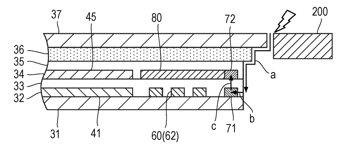
[0065]FIG. 8 depicts the touch panel according to the present invention. Portions corresponding to the component elements of the touch panel 100 depicted in FIGS. 2A to 4C are identified with the same reference numerals and detailed descriptions thereof are omitted.
[0066]In a touch panel 300 depicted in FIG. 8, a space is provided as depicted in FIG. 8 between shielding wiring 80′ indicated by hatching and the second outer ground wiring lines 72, whereby the shielding wiring 80′ is separated and insulated from the second outer ground wiring lines 72. In addition, the shielding wiring 80′ is connected to the ground wiring lines 63 for separation of transmission and reception wiring. In the insulating layer 33, holes 91 indicated by dashed lines in FIG. 8 are provided, and, in the positions of the holes 91, the shielding wiring 80′ is connected to the ground wiring lines 63 for separation of transmission and reception wiring.
[0067]With such a structure, it is possible to prevent the s...
second embodiment
[0068]Next, the touch panel according to the present invention will be described with reference to FIG. 9.
[0069]In the touch panel 300 of the above-described first embodiment, as is the case with the touch panel 100 depicted in FIG. 2B, the second outer ground wiring lines 72 are located above the first outer ground wiring lines 71, with the insulating layer 33 placed therebetween. However, in a touch panel 400 of the second embodiment, the first outer ground wiring lines 71 and the second outer ground wiring lines 72 are formed by overprinting and therefore the insulating layer 33 is not interposed between the first outer ground wiring lines 71 and the second outer ground wiring lines 72. It is simply necessary to perform overprinting by setting (limiting) the position in which the insulating layer 33 is formed by printing such that, as depicted in FIG. 9, the first outer ground wiring lines 71 are not covered with the insulating layer 33, and the second outer ground wiring lines 7...
PUM
 Abstract
Description
Claims
Application Information
 - Generate Ideas
- Intellectual Property
- Life Sciences
- Materials
- Tech Scout
- Unparalleled Data Quality
- Higher Quality Content
- 60% Fewer Hallucinations
Browse by: Latest US Patents, China's latest patents, Technical Efficacy Thesaurus, Application Domain, Technology Topic, Popular Technical Reports.
© 2025 PatSnap. All rights reserved.Legal|Privacy policy|Modern Slavery Act Transparency Statement|Sitemap|About US| Contact US: help@patsnap.com