Method to prevent loss of data of a transistor-based memory unit

Active Publication Date: 2017-03-30
EGALAX EMPIA TECH INC
View PDF1 Cites 0 Cited by
  • Summary
  • Abstract
  • Description
  • Claims
  • Application Information

AI Technical Summary

Benefits of technology

[0009]The present invention has been accomplished under the circumstances in view. It is therefore the main object of the present invention to p

Problems solved by technology

Thus, when writing new memory cell information into the floating gate (FG), it will be

Method used


Image

  • Method to prevent loss of data of a transistor-based memory unit
  • Method to prevent loss of data of a transistor-based memory unit
  • Method to prevent loss of data of a transistor-based memory unit

Examples


Example

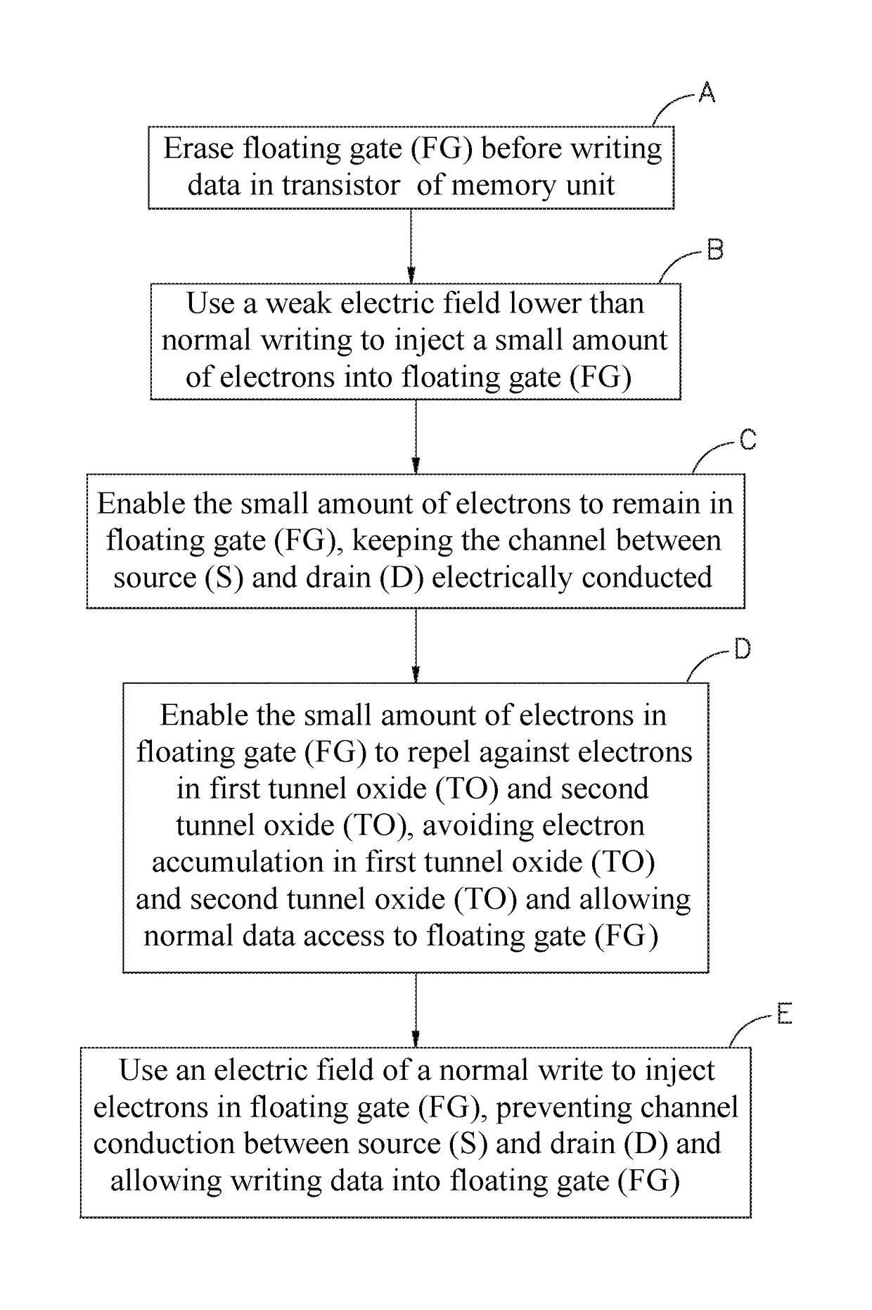
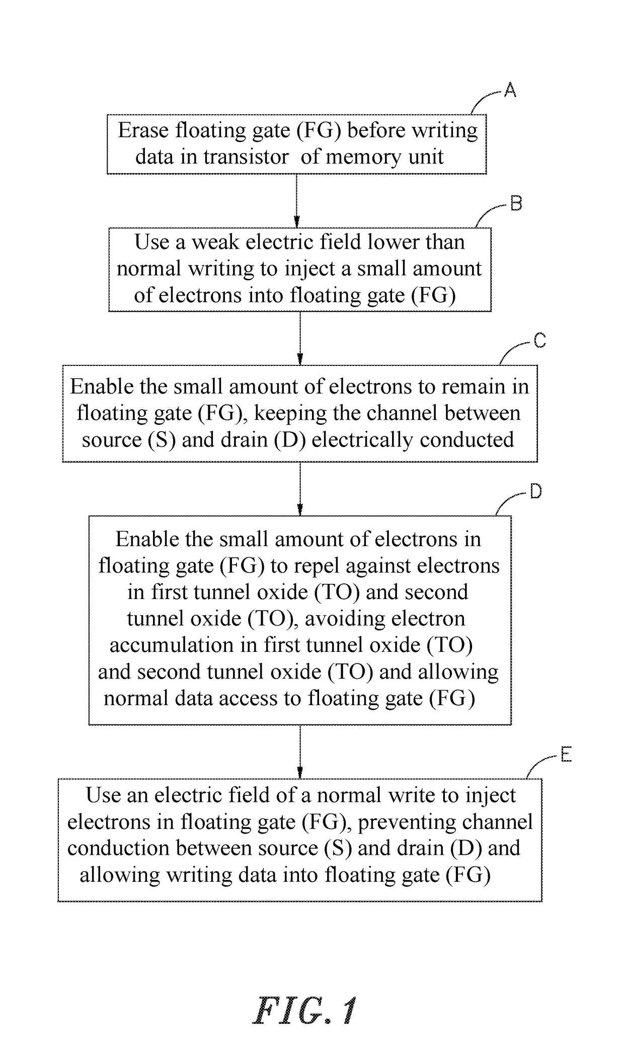
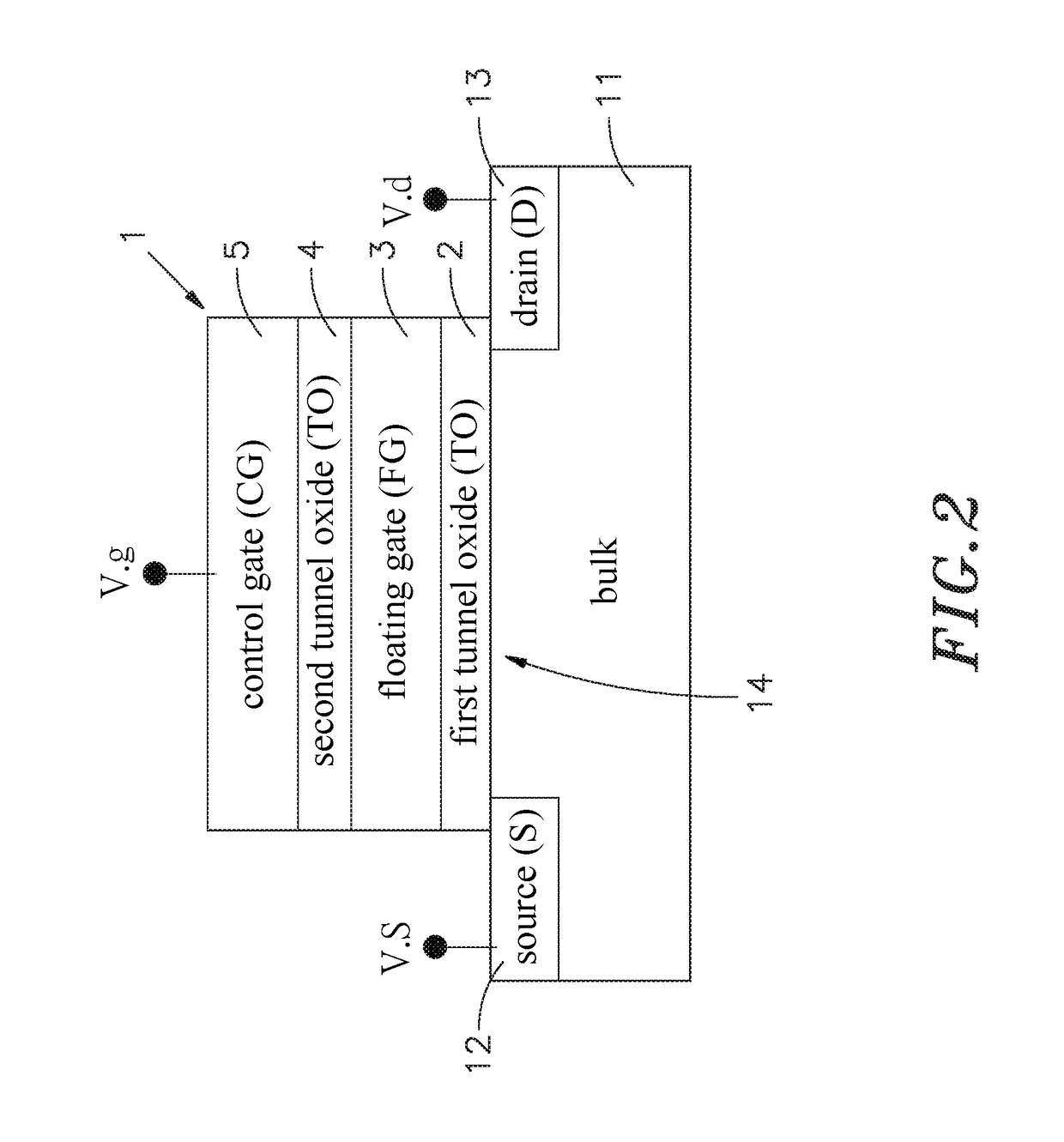
[0017]Referring to FIGS. 1 and 2, a flow chart of the present invention and a sectional side view illustrating the structure of a memory unit in accordance with the present invention are shown. As illustrated in the best mode of the present invention, a transistor 1 of the memory unit (for example, flash memory) comprises a bulk 11, a source (S) 12 and a drain (D) 13 formed on the bulk 11, a channel 14 in communication between the source (S) 12 and the drain (D) 13, and a first tunnel oxide (TO) 2, a floating gate (FG) 3, a second tunnel oxide (TO) 4 and a control gate (CG) 5 stacked up on the channel 14 in a proper order in such a manner that the first tunnel oxide (TO) 2 is formed between the bulk 11 and one side of the floating gate (FG) 3; the second tunnel oxide (TO) 4 is formed between an opposite side of the floating gate (FG) 3 and the control gate (CG) 5. The method to prevent loss of data in the memory unit comprises the steps of:

[0018](A) Erase the floating gate (FG) 3 be...


PUM


Abstract

A method to prevent loss of data of transistor-based memory unit including bulk, source and drain formed on bulk and first tunnel oxide, floating gate, second tunnel oxide and control gate stacked up on channel between source and drain is disclosed to include steps of: erasing the floating gate, using weak electric field inject small amount of electrons into floating gate, enabling small amount of electrons to remain in floating gate to keep channel between source and drain electrically conducted, enabling small amount of electrons in floating gate to repel against electrons in first tunnel oxide and second tunnel oxide so as avoid electron accumulation in first tunnel oxide and second tunnel oxide and allow normal data access floating gate, and using electric field of normal write to inject electrons in floating gate so as to prevent channel conduction between source and drain and allow writing data into floating gate.

Description

[0001]This reference is based on Provisional Application Ser. No. 62 / 234,887, filed on Sep. 30, 2015, currently pending.BACKGROUND OF THE INVENTION[0002]1. Field of the Invention[0003]The present invention relates to a touch-sensing input device and more particularly, to a method to prevent loss of data of a transistor-based memory unit is achieved by: erasing the floating gate (FG) and injecting a small amount of electrons into the floating gate (FG) to avoid electron accumulation in the first tunnel oxide (TO) and the second tunnel oxide (TO) and to allow normal data access to the floating gate (FG), and then using an electric field of a normal write to inject electrons in the floating gate (FG) to prevent channel conduction between the source (S) and the drain (D) and to allow writing data into the floating gate (FG), thereby reducing the possibility of a read error.[0004]2. Description of the Related Art[0005]A memory is a semiconductor component for storing electronic informati...

Claims


Application Information

Patent Timeline
IPC IPC(8): G11C16/04G11C16/14H01L29/788G11C16/10
CPCG11C16/0408H01L29/7883G11C16/14G11C16/10G11C7/24G11C16/22G11C16/3409
Inventor LIN, GUANG-HUEI
Owner EGALAX EMPIA TECH INC
Why Eureka
Try Eureka