Insulator film formation method by flexographic printing and flexographic printing plate

Active Publication Date: 2017-04-27
JAPAN AVIATION ELECTRONICS IND LTD
View PDF10 Cites 0 Cited by
  • Summary
  • Abstract
  • Description
  • Claims
  • Application Information

AI Technical Summary

Benefits of technology

The invention can prevent a protrusion from occurring in the thickness of a film around the edge of a printing pattern.

Problems solved by technology

When in the insulator film there is a protrusion around the through hole that is used for connecting the two conductor films, in other words, used for conductor joining and thus the film thickness of the insulator film is large thereat, a conductor joining failure is caused.
For this reason, on the parts surrounded by broken lines in FIG. 3B, defects of the second conductor film 24 which raise problems of electrical conduction continuity are generated, that is, poor electrical connection between the two conductor films due to breaks is generated.

Method used


Image

  • Insulator film formation method by flexographic printing and flexographic printing plate
  • Insulator film formation method by flexographic printing and flexographic printing plate
  • Insulator film formation method by flexographic printing and flexographic printing plate

Examples


Embodiment Construction

[0032]An embodiment of the present invention will be described on the basis of a working example with reference to the drawings.

[0033]FIG. 4A illustrates a structure of a flexographic printing plate of an embodiment according to the present invention. In FIG. 4A, only a convex portion 31 defining a printing pattern of the flexographic printing plate is illustrated and illustration of halftone dots convexly formed on the convex portion 31 is omitted.

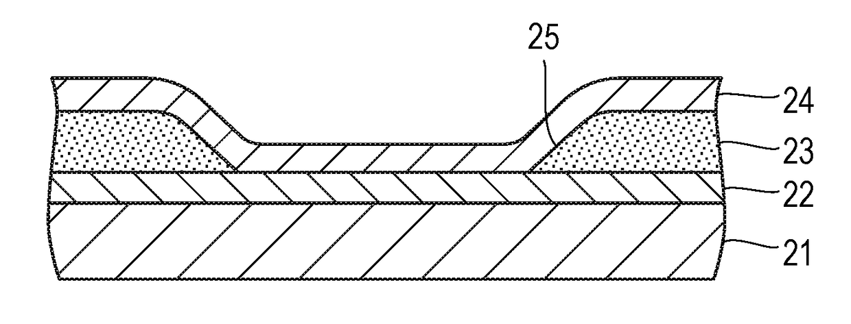
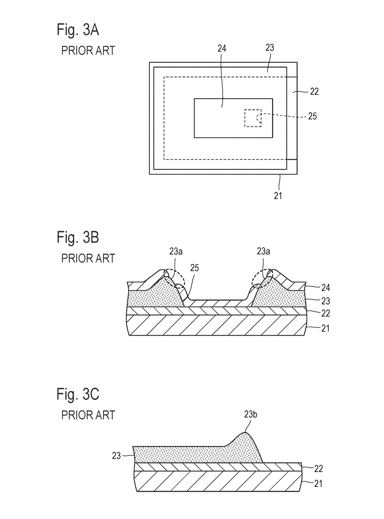
[0034]The convex portion 31 of the flexographic printing plate illustrated in FIG. 4A is designed to form an insulator film 23 illustrated in FIG. 3A described above. In this example, halftone dot condition change regions 41 and 42 are provided on the convex portion 31, in which conditions of halftone dots for transferring an ink as an insulator film material, such as polyimide, epoxy resin, or acrylic resin, from an anilox roll to a printing object are varied relative to other region on the convex portion 31. It should be noted that, in ...


PUM


Abstract

A method of forming an insulator film by flexographic printing is provided with which an insulator film is formed on a printing object by using ink as an insulator film material and a flexographic printing plate with halftone dots convexly formed on a convex portion thereof that defines a printing pattern. A halftone dot condition change region with a condition of the halftone dots varied such that an ink retention volume therein is smaller than that in other region on the convex portion is provided on a part of the convex portion corresponding to an edge of the printing pattern.

Description

TECHNICAL FIELD[0001]The present invention relates to a method of forming an insulator film by flexographic printing and a flexographic printing plate used in the method.BACKGROUND ART[0002]If not vacuum processing such as sputtering but a printing process can be used in a process of forming a film such as an insulator film or a conductor film, not only improvement in productivity but also cost reduction due to unnecessity of an expensive film forming apparatus will be expected.[0003]Japanese Patent Application Laid Open No. 2001-51259 (hereinafter referred to as “Patent Literature 1”) discloses that, in a substrate used for a liquid crystal device, a surface protection film which is an insulator film covering an electrode pattern formed as a conductor film on the substrate is formed by flexographic printing. FIGS. 1A, 1B, 2A, and 2B illustrate an insulator film formed by flexographic printing as disclosed in Patent Literature 1. In FIGS. 1A, 1B, 2A, and 2B, reference numeral 11 rep...

Claims


Application Information

Patent Timeline
IPC IPC(8): B41F19/00B41N1/16
CPCB41N1/16B41F19/001B41M3/00B41N1/12B41M1/04B41N1/22G06F3/0446G06F3/0445B41P2200/12G06F2203/04103B41F5/24G02F1/1337G02F1/13378B41P2217/50G02F1/1303B41N1/00B41M1/26B41M3/006
Inventor SAKAUE, AKITOSHIIWAO, NAOKISATO, MITSUNORITAKEZAWA, YUTAKAKOGAWA, YUTARONAITO, MITSUTOSHI
Owner JAPAN AVIATION ELECTRONICS IND LTD
Why Eureka
Try Eureka