Supercharge Your Innovation With Domain-Expert AI Agents!

NAND flash memory and program method thereof

a technology of flash memory and program method, applied in the field of nand flash memory, can solve the problems that the influence caused by the floating gate (fg) coupling between memory cells also becomes non-ignorable, and achieve the effect of suppressing the influence and high reliability

Active Publication Date: 2017-05-18
WINBOND ELECTRONICS CORP
View PDF2 Cites 4 Cited by
  • Summary
  • Abstract
  • Description
  • Claims
  • Application Information

AI Technical Summary

Benefits of technology

This patent is about a new method for NAND flash memory that solves the problems of the related art. It reduces the influence of neighboring memory cells, resulting in a narrower threshold distribution range and higher reliability of the flash memory. The method involves soft-programming the adjacent memory cells to minimize the FG coupling effect.

Problems solved by technology

Along with propulsion of the low voltage and high integration of the flash memory, besides the capacitance coupling between the bit lines, the influence caused by floating gate (FG) coupling between memory cells also becomes non-ignorable.

Method used


Image

  • NAND flash memory and program method thereof
  • NAND flash memory and program method thereof
  • NAND flash memory and program method thereof

Examples


Embodiment Construction

[0022]Embodiments of the invention are described below with reference of provided figures. Moreover, it should be noted that in the figures, the figures referred to herein are drawn for clarity of illustration and are not necessarily drawn to scale.

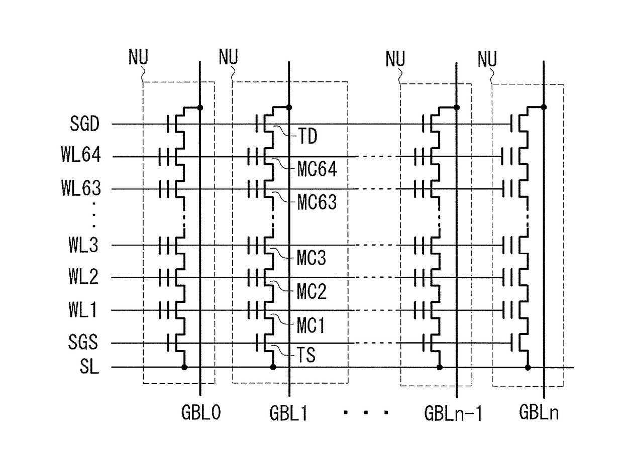
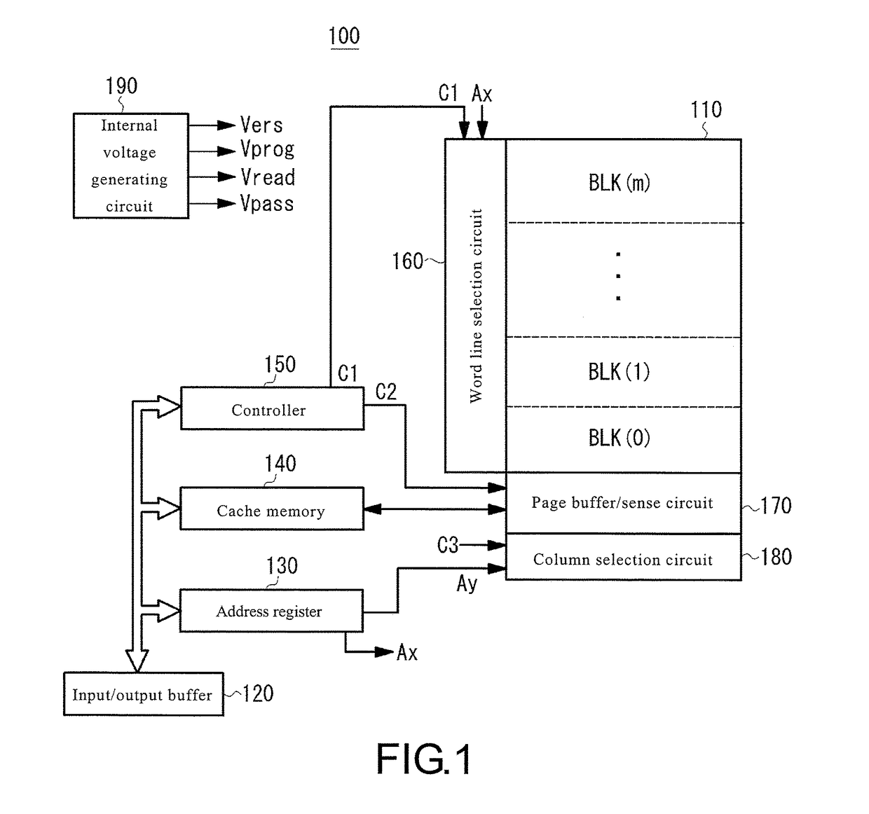
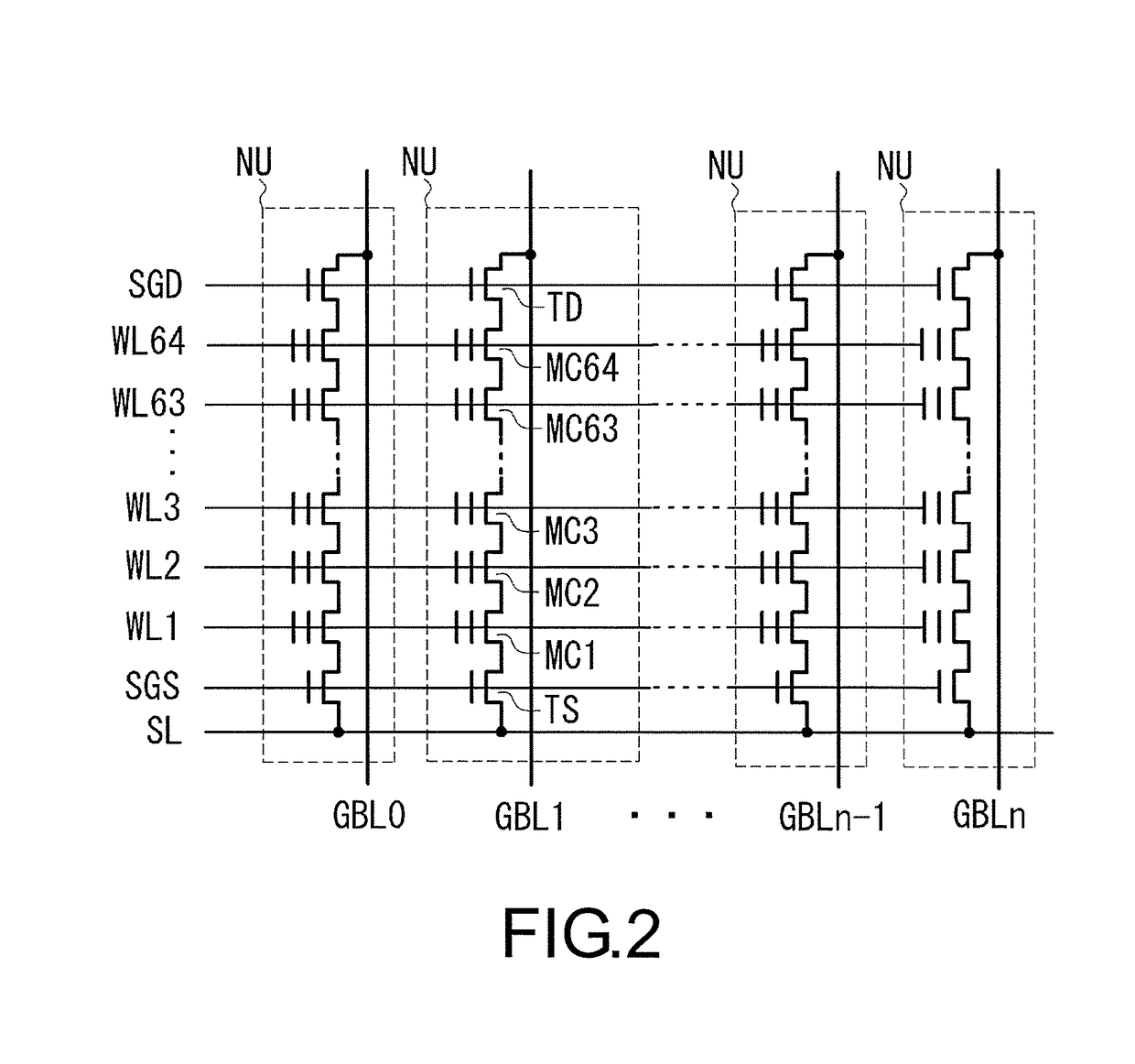
[0023]As shown in FIG. 1, the flash memory 100 includes a memory array 110, which is formed with a plurality of memory cells arranged in an array; an input / output buffer 120, which is connected to an external input / output terminal I / O; an address register 130, which receives address data coming from the input / output buffer 120; a cache memory 140, which keeps input / output data; a controller 150, which generates control signals C1, C2, C3, etc., where the control signals C1, C2, C3, etc., control each part based on command data coming from the input / output buffer 120 and external control signals (chip enable (CE), command latch enable (CLE), address latch enable (ALE), ready / busy (RY / BY), etc., that are not shown); a word line selection ci...


PUM


Abstract

A NADN flash memory and a program method thereof suppressing an influence caused by FG coupling and having a high reliability are provided. The program method of the flash memory of the present invention includes a step of selecting pages of a memory array, a step of applying a programming voltage to even-numbered pages of the selected pages, a step of soft-programming odd-numbered pages of the selected pages and a step of applying the programming voltage to the odd-numbered pages after the programming of the even-numbered pages is completed.

Description

CROSS-REFERENCE TO RELATED APPLICATION[0001]This application claims the priority benefit of Japan application serial no. 2015-225308, filed on Nov. 18, 2015. The entirety of the above-mentioned patent application is hereby incorporated by reference herein and made a part of this specification.BACKGROUND OF THE INVENTION[0002]Field of the Invention[0003]The invention relates to a NAND flash memory, and particularly relates to a program method of selected pages.[0004]Description of Related Art[0005]In a NAND flash memory, when a page is read or programmed, in order to suppress a noise caused by capacitance coupling between bit lines, one word line separately operates for even-numbered pages and odd-numbered pages. For example, when the even-numbered page is read, the odd-numbered page is grounded, and when the odd-numbered page is read, the even-numbered page is grounded; and when the even-numbered page is programmed, programming of the odd-numbered page is disabled, and when the odd-...

Claims


Application Information

Patent Timeline
Patent Type & Authority Applications(United States)
IPC IPC(8): G11C16/10G11C16/34
CPCG11C16/3459G11C16/10G11C16/3409G11C16/0483G11C16/3404
Inventor YANO, MASARU
Owner WINBOND ELECTRONICS CORP
Features
  • R&D
  • Intellectual Property
  • Life Sciences
  • Materials
  • Tech Scout
  • Unparalleled Data Quality
  • Higher Quality Content
  • 60% Fewer Hallucinations
Learn More